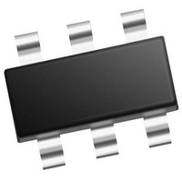
MCP4706A3T-E/CH Microchip Technology, MCP4706A3T-E/CH Datasheet - Page 44

MCP4706A3T-E/CH
Manufacturer Part Number
MCP4706A3T-E/CH
Description
Single, 8-bit NV DAC With Ext Vref And I2C Interface 6 SOT-23 T/R
Manufacturer
Microchip Technology
Series
-r
Datasheet
1.MCP4706A0T-ECH.pdf
(86 pages)
Specifications of MCP4706A3T-E/CH
Number Of Converters
1
Conversion Rate
1
Resolution
8 bit
Interface Type
I2C
Settling Time
6 us
Supply Voltage (max)
5.5 V
Supply Voltage (min)
2.7 V
Maximum Operating Temperature
+ 125 C
Mounting Style
SMD/SMT
Package / Case
SOT-23-6
Maximum Power Dissipation
452 mW
Minimum Operating Temperature
- 40 C
Supply Current
210 uA
Number Of Bits
8
Data Interface
EEPROM, I²C, Serial
Voltage Supply Source
Single Supply
Power Dissipation (max)
452mW
Operating Temperature
-40°C ~ 125°C
Mounting Type
Surface Mount
Number Of Outputs And Type
*
Lead Free Status / Rohs Status
Details
MCP4706/4716/4726
5.3
The MCP47X6’s I
NXP I
module’s features:
• 7-bit slave addressing
• Supports three clock rate modes:
• Support Multi-Master Applications
• General call addressing (Reset and Wake-Up
The I
The NXP I
field lengths, timings, etc. of a frame. The frame
content defines the behavior of the device. The frame
content for the MCP47X6 is defined in Section 6.0.
5.3.1
Figure 5-8
clock is generated by the master. The following
definitions are used for the bit states:
• Start bit (S)
• Data bit
• Acknowledge (A) bit (driven low) /
• Repeated Start bit (Sr)
• Stop bit (P)
5.3.1.1
The Start bit (see
a data transfer sequence. The Start bit is defined as the
SDA signal falling when the SCL signal is “High”.
FIGURE 5-2:
5.3.1.2
The SDA signal may change state while the SCL signal
is Low. While the SCL signal is High, the SDA signal
MUST be stable (see
FIGURE 5-3:
DS22272A-page 44
SDA
SCL
SDA
SCL
- Standard mode, clock rates up to 100 kHz
- Fast mode, clock rates up to 400 kHz
- High-speed mode (HS mode), clock rates up
commands)
No Acknowledge (A) bit (not driven low)
to 3.4 MHz
2
2
C 10-bit addressing mode is not supported.
C specification. The following lists some of the
I
2
2
S
shows the I
C Operation
C specification only defines the field types,
I
2
C BIT STATES AND SEQUENCE
Start Bit
Data Bit
Figure
2
C module is compatible with the
Figure
2
Start Bit.
Data Bit.
C transfer sequence. The serial
5-2) indicates the beginning of
1st Bit
5-5).
Data Bit
1st Bit
2nd Bit
2nd Bit
5.3.1.3
The A bit (see
the receiving device to the transmitting device.
Depending on the context of the transfer sequence, the
A bit may indicate different things. Typically the Slave
device will supply an A response after the Start bit and
8 “data” bits have been received. An A bit has the SDA
signal low.
FIGURE 5-4:
Not A (A) Response
The A bit has the SDA signal high.
some of the conditions where the Slave Device will
issue a Not A (A).
If an error condition occurs (such as an A instead of A),
then a START bit must be issued to reset the command
state machine.
TABLE 5-1:
General Call
Slave Address
valid
Slave Address
not valid
Communication
during
EEPROM write
cycle
Bus Collision
SDA
SCL
Event
Acknowledge (A) Bit
Figure
8
D0
MCP47X6 A / A RESPONSES
Acknowledge
Response
5-4) is typically a response from
Acknowledge Waveform.
© 2011 Microchip Technology Inc.
N.A.
Bit
A
A
A
A
After device has
received address
and command,
and valid
conditions for
EEPROM write
I
Resets, or a
“Don’t Care” if
the collision
occurs on the
Master’s “Start
bit”
2
C Module
Table 5-1
Comment
9
A
shows


