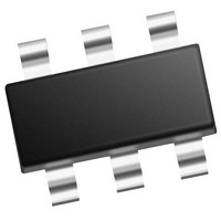
MCP4706A3T-E/CH Microchip Technology, MCP4706A3T-E/CH Datasheet - Page 6

MCP4706A3T-E/CH
Manufacturer Part Number
MCP4706A3T-E/CH
Description
Single, 8-bit NV DAC With Ext Vref And I2C Interface 6 SOT-23 T/R
Manufacturer
Microchip Technology
Series
-r
Datasheet
1.MCP4706A0T-ECH.pdf
(86 pages)
Specifications of MCP4706A3T-E/CH
Number Of Converters
1
Conversion Rate
1
Resolution
8 bit
Interface Type
I2C
Settling Time
6 us
Supply Voltage (max)
5.5 V
Supply Voltage (min)
2.7 V
Maximum Operating Temperature
+ 125 C
Mounting Style
SMD/SMT
Package / Case
SOT-23-6
Maximum Power Dissipation
452 mW
Minimum Operating Temperature
- 40 C
Supply Current
210 uA
Number Of Bits
8
Data Interface
EEPROM, I²C, Serial
Voltage Supply Source
Single Supply
Power Dissipation (max)
452mW
Operating Temperature
-40°C ~ 125°C
Mounting Type
Surface Mount
Number Of Outputs And Type
*
Lead Free Status / Rohs Status
Details
MCP4706/4716/4726
ELECTRICAL CHARACTERISTICS (CONTINUED)
DS22272A-page 6
Electrical Specifications: Unless otherwise indicated, V
= -40°C to +125°C. Typical values at +25°C.
Output Amplifier
Minimum Output Volt-
age
Maximum Output
Voltage
Phase Margin
Slew Rate
Short Circuit Current
Settling Time
Power Down Output
Disable Time Delay
Power Down Output
Enable Time Delay
External Reference (V
Input Range
Input Impedance
Input Capacitance
-3 dB Bandwidth
Total Harmonic Distor-
tion
Dynamic Performance
Major Code Transition
Glitch
Digital Feedthrough
Note 1:
Parameters
2:
3:
4:
5:
6:
7:
This parameter is ensured by design and is not 100% tested.
This gain error does not include offset error. See Section 2 for more details in plots.
Within 1/2 LSb of final value when code changes from 1/4 to 3/4 of FSR. (Example: 400h to C00h in 12- bit device).
The power-up ramp rate affects on uploading the EEPROM contents to the DAC register. It measures the rise of V
over time.
This parameter is ensured by characterization, and not 100% tested.
The PD1:PD0 = ‘10’, and ‘11’ configurations should have the same current.
V
DD
= 5.5V.
REF
(Note
V
V
t
)
Symbol
SETTLING
OUT(MAX)
OUT(MIN)
R
C_
T
T
V
THD
PM
SR
I
(Note
VREF
PDD
PDE
REF
SC
REF
1)
1)
0.04
Min
—
—
—
—
—
—
—
—
—
—
—
—
—
—
7
0
Typical
V
0.55
0.01
0.04
10.5
86.5
67.7
<10
210
-73
DD
66
15
29
45
—
—
DD
6
1
–
= 2.7V to 5.5V, V
V
Max
0.04
V
24
—
—
—
—
—
—
—
DD
—
—
—
—
—
—
—
DD
-
Degree
Units
SS
V/µs
nV-s
nV-s
kHz
kHz
mA
kΩ
dB
pF
(°)
µs
µs
µs
V
V
V
V
= 0V, R
Output Amplifier’s minimum drive
Output Amplifier’s maximum drive
C L = 400 pF, R L = ∞
Note 3
PD1:PD0 = “00” -> ‘11’, ‘10’, or ‘01’
started from falling edge SCL at end of
ACK bit.
V
connected.
PD1:PD0 = ‘11’, ‘10’, or ‘01’ -> “00”
started from falling edge SCL at end of
ACK bit.
Volatile DAC Register = FFh,
V
Buffered Mode
Unbuffered Mode
Unbuffered Mode
Unbuffered Mode
V
V
V
V
V
V
Frequency = 1 kHz
1 LSb change around major carry
(800h to 7FFh)
L
OUT
OUT
REF
REF1
REF
REF1
REF
REF1
= 5 kΩ from V
= 2.048V ± 0.1V,
= 2.048V ± 0.1V,
= 2.048V ± 0.1V,
= V
= 10 mV. V
:V
:V
:V
REF0
REF0
REF0
OUT
© 2011 Microchip Technology Inc.
= ‘10’, G = ‘0’
= ‘10’, G = ‘1’
= ‘10’, G = ‘0’,
OUT
- 10 mV. V
Conditions
OUT
to GND, C L = 100 pF, T
not connected.
OUT
not
DD
A


