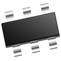
MCP4706A3T-E/CH Microchip Technology, MCP4706A3T-E/CH Datasheet - Page 37

MCP4706A3T-E/CH
Manufacturer Part Number
MCP4706A3T-E/CH
Description
Single, 8-bit NV DAC With Ext Vref And I2C Interface 6 SOT-23 T/R
Manufacturer
Microchip Technology
Series
-r
Datasheet
1.MCP4706A0T-ECH.pdf
(86 pages)
Specifications of MCP4706A3T-E/CH
Number Of Converters
1
Conversion Rate
1
Resolution
8 bit
Interface Type
I2C
Settling Time
6 us
Supply Voltage (max)
5.5 V
Supply Voltage (min)
2.7 V
Maximum Operating Temperature
+ 125 C
Mounting Style
SMD/SMT
Package / Case
SOT-23-6
Maximum Power Dissipation
452 mW
Minimum Operating Temperature
- 40 C
Supply Current
210 uA
Number Of Bits
8
Data Interface
EEPROM, I²C, Serial
Voltage Supply Source
Single Supply
Power Dissipation (max)
452mW
Operating Temperature
-40°C ~ 125°C
Mounting Type
Surface Mount
Number Of Outputs And Type
*
Lead Free Status / Rohs Status
Details
4.4
The DAC output is buffered with a low power and
precision output amplifier (op amp).
a block diagram.
This amplifier provides a rail-to-rail output with low
offset voltage and low noise. The user can select the
output gain of the output amplifier. Gain options are:
a)
b)
The amplifier’s output can drive the resistive and high
capacitive loads without oscillation. The amplifier
provides a maximum load current which is enough for
most programmable voltage reference applications.
Refer to
the specifications of the output amplifier.
In any of the three Power-Down modes, the op amp is
powered down and it’s output becomes a high
impedance to the V
FIGURE 4-4:
Diagram.
4.4.1
The amplifier’s gain is controlled by the Gain (G)
configuration bit (See
selection. When the V
device’s V
1 is used. The volatile G bit value can be modified by:
• POR event
• BOR event
• I
• I
© 2011 Microchip Technology Inc.
Note:
2
2
C write commands
C General Call Reset command
Gain of 1, with either V
reference voltage
Gain of 2, only when V
reference voltage. The V
be limited to V
Section 1.0 “Electrical Characteristics”
Output Buffer / V
DD
V
The load resistance must keep higher
than 5 kΩ for the stable and expected
analog
specifications).
PROGRAMMABLE GAIN
W
voltage, the G bit is ignored and a gain of
Gain (1x or 2x)
(G = 0 or 1)
Op
Amp
DD
OUT
/2.
output
Table
Output Buffer Block
pin.
RL
reference selection is the
4-4) and the V
DD
REF
(to
REF
OUT
or V
pin voltage should
REF
pin is used as
meet
Operation
Figure 4-4
pin used as
RL
electrical
reference
V
OUT
shows
for
4.4.2
The volatile DAC Register’s value controls the analog
V
bits. The volatile DAC Register’s value is unsigned
binary.
The formula for the output voltage is given in
Equation
DAC Register values and the corresponding theoretical
V
EQUATION 4-1:
The DAC register value will be latched on the falling
edge of the acknowledge pulse of the write command’s
last byte. Then the V
new value.
The following events update the analog voltage output
(V
• Power-On-Reset or General Call Reset
• Falling edge of the acknowledge pulse of the last
4.4.2.1
The Step voltage is dependent on the device resolution
and the output voltage range. One LSb is defined as
the ideal voltage difference between two successive
codes. The step voltage can easily be calculated by
using
equal to 1.
4.4.3
The V
in parallel with a 5 kΩ resistive load (to meet electrical
specifications).
Resistive Load.
V
after about 3.5 kΩ. It is recommended to use a load
with R
# Resistors in Resistor Ladder = 4096 (MCP4726)
OUT
OUT
OUT
MCP4706/4716/4726
Note:
OUT
command: Output is updated with EEPROM data.
write command byte.
V
OUT
voltage, along with the device’s five configuration
voltage for the MCP47X6 devices.
):
OUT
Equation 4-1
drops slowly as the load resistance decreases
L
greater than 5 kΩ.
=
4-1.
pin can drive up to 100 pF of capacitive load
OUTPUT VOLTAGE
When Gain = 2 (V
if V
limited to V
V
DAC Register values mid-scale and
greater, since the op amp at full scale
output.
DRIVING RESISTIVE AND
CAPACITIVE LOADS
# Resistors in Resistor Ladder
OUT
Resolution / Step Voltage
V
Table 4-1
REF
RL
Figure 2-57
voltage will not change for volatile
* DAC Register Value
> V
where the DAC Register Value is
OUT
DD
CALCULATING OUTPUT
VOLTAGE (V
DD
voltage will start driving to the
shows examples of volatile
. So if V
/ 2, the V
RL
shows the V
= V
REF
1024 (MCP4716)
256 (MCP4706)
OUT
REF
DS22272A-page 37
OUT
= V
voltage will be
),
DD
)
, then the
* Gain
OUT
vs.


