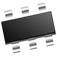
MCP4706A3T-E/CH Microchip Technology, MCP4706A3T-E/CH Datasheet - Page 41

MCP4706A3T-E/CH
Manufacturer Part Number
MCP4706A3T-E/CH
Description
Single, 8-bit NV DAC With Ext Vref And I2C Interface 6 SOT-23 T/R
Manufacturer
Microchip Technology
Series
-r
Datasheet
1.MCP4706A0T-ECH.pdf
(86 pages)
Specifications of MCP4706A3T-E/CH
Number Of Converters
1
Conversion Rate
1
Resolution
8 bit
Interface Type
I2C
Settling Time
6 us
Supply Voltage (max)
5.5 V
Supply Voltage (min)
2.7 V
Maximum Operating Temperature
+ 125 C
Mounting Style
SMD/SMT
Package / Case
SOT-23-6
Maximum Power Dissipation
452 mW
Minimum Operating Temperature
- 40 C
Supply Current
210 uA
Number Of Bits
8
Data Interface
EEPROM, I²C, Serial
Voltage Supply Source
Single Supply
Power Dissipation (max)
452mW
Operating Temperature
-40°C ~ 125°C
Mounting Type
Surface Mount
Number Of Outputs And Type
*
Lead Free Status / Rohs Status
Details
TABLE 4-3:
TABLE 4-4:
TABLE 4-5:
REGISTER 4-1:
© 2011 Microchip Technology Inc.
Note 1:
Note 1:
POR Event
BOR Event
POR/BOR Event
Bit Name
V
REF
RDY/BSY
PD1:PD0
Bit Name
Name
Name
2:
POR
1:V
G
REF
Default configuration when the device is shipped to customer. The POR/BOR value may be modified by
writing the corresponding nonvolatile configuration bit.
Default configuration when the device is shipped to customer. The POR/BOR value may be modified by
writing the corresponding nonvolatile configuration bit.
This device does not implement this bit, so there is no corresponding POR/BOR value.
VREF1
0
R/W
0
0
(1)
STATUS BITS OPERATION
CONFIGURATION BITS
CONFIGURATION BIT VALUES AFTER POR/BOR EVENT
Function
This bit indicates the state of the EEPROM program memory
1 = EEPROM is not in a programming cycle
0 = EEPROM is in a programming cycle
Power-On-Reset status indicator (flag)
1 = Device is powered on with V
0 = Device is in powered off state. If this value is read, V
Function
Resistor Ladder Voltage Reference (V
0x = V
10 = V
11 = V
Power-Down selection bits
When the DAC is powered down, most of the internal circuits are powered off and the op amp is
disconnected from the V
00 = Not Powered Down (Normal operation)
01 = Powered Down - V
10 = Powered Down - V
11 = Powered Down - V
Gain selection bit
0 =
1 =
—
—
R/W
D11
0
Note:
Note:
(1)
DAC REGISTER BITS
(2)
(2)
VREF0
Ensure that V
Unreliable device operation should be expected.
R/W
1x (gain of 1)
2x (gain of 2). Not applicable when V
0
0
DD
REF
REF
(1)
R/W
—
—
D10
0
(1)
(2)
(2)
(Unbuffered)
See
If V
setting.
pin (Unbuffered)
pin (Buffered)
REF
R/W
—
0
R/W
PD1
Table 4-2
D9
D9
0
(1)
1
(1)
(2)
DD
= V
is above V
DD
R/W
—
0
D8
D8
(1)
OUT
(2)
, the device uses a gain of 1 only, regardless of the gain selection bit (G)
OUT
OUT
OUT
R/W
PD0
and
0
1
(1)
pin.
is loaded with 1 kΩ resistor to ground.
is loaded with 100 kΩ resistor to ground.
is loaded with 500 kΩ resistor to ground.
R/W
0
Figure 4-5
D7
D7
D7
(1)
DD(MIN)
DD
R/W
0
G
0
> V
(1)
R/W
0
D6
D6
D6
RL
(1)
POR
to ensure proper operation.
) selection bits
for more details.
When V
When V
Comment
DD
R/W
.
0
D5
D5
D5
MCP4706/4716/4726
(1)
is used as V
DD
DD
R/W
0
D4
D4
D4
(1)
transitions from V
transitions from V
DD
R/W
RL
0
D3
D3
D3
(1)
< V
DD(MIN)
R/W
0
D2
D2
D2
(1)
DD
DD
< V
R/W
0
D1
D1
D1
< V
> V
(1)
POR
POR
BOR
.
R/W Comment
DS22272A-page 41
0
D0
D0
D0
(1)
to V
to V
DD
DD
MCP4706
MCP4716
MCP4726
> V
< V
POR
BOR


