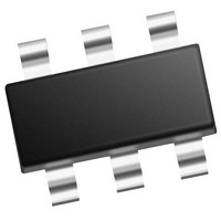
MCP4706A3T-E/CH Microchip Technology, MCP4706A3T-E/CH Datasheet - Page 66

MCP4706A3T-E/CH
Manufacturer Part Number
MCP4706A3T-E/CH
Description
Single, 8-bit NV DAC With Ext Vref And I2C Interface 6 SOT-23 T/R
Manufacturer
Microchip Technology
Series
-r
Datasheet
1.MCP4706A0T-ECH.pdf
(86 pages)
Specifications of MCP4706A3T-E/CH
Number Of Converters
1
Conversion Rate
1
Resolution
8 bit
Interface Type
I2C
Settling Time
6 us
Supply Voltage (max)
5.5 V
Supply Voltage (min)
2.7 V
Maximum Operating Temperature
+ 125 C
Mounting Style
SMD/SMT
Package / Case
SOT-23-6
Maximum Power Dissipation
452 mW
Minimum Operating Temperature
- 40 C
Supply Current
210 uA
Number Of Bits
8
Data Interface
EEPROM, I²C, Serial
Voltage Supply Source
Single Supply
Power Dissipation (max)
452mW
Operating Temperature
-40°C ~ 125°C
Mounting Type
Surface Mount
Number Of Outputs And Type
*
Lead Free Status / Rohs Status
Details
MCP4706/4716/4726
8.3.1.2
When calibrating a set point or threshold of a sensor,
typically only a small portion of the DAC output range is
utilized. If the LSb size is adequate enough to meet the
application’s accuracy needs, the unused range is
sacrificed without consequences. If greater accuracy is
needed, then the output range will need to be reduced
to increase the resolution around the desired threshold.
If the threshold is not near V
creating a “window” around the threshold has several
advantages. One simple method to create this
“window” is to use a voltage divider network with a
pull-up and pull-down resistor.
6
FIGURE 8-4:
DAC.
EQUATION 8-2:
DS22272A-page 66
2-wire
I
Optional
2
illustrate this concept.
V
C™
V
V
MCP47X6
OUT
TRIP
REF
Thevenin
Equivalent
= V
V
=
DD
REF
V
-------------------------------------------- -
Building a “Window” DAC
OUT
R
V
• G •
R
SENSE
R
OUT
1
23
+
R
+
1
R
V
Single-Supply “Window”
V
CALCULATIONS
DAC Register Value
R
V
23
V
OUT
OUT
23
23
23
R
R
R
=
=
3
2
V
1
REF
AND V
V
CC
------------------ -
R
(
------------------------------------------------------
Figure 8-4
R
V
R
2
CC
2
, 2 • V
CC+
1
–
N
2
+
R
+
V
R
3
R
TRIP
3
R
V
C
TRIP
2
REF
23
2
)
1
+
+
and
Comp.
R
, or V
R
(
23
V
V
3
V
V
CC
CC-
CC
Figure 8-
TRIP
SS
+
–
R
3
then
)
V
O
8.4
Bipolar operation is achievable by utilizing an external
operational amplifier. This configuration is desirable
due to the wide variety and availability of op amps. This
allows a general purpose DAC, with its cost and
availability advantages, to meet almost any desired
output voltage range, power and noise performance.
Figure 8-5
configuration. R
while R
offset. Note that R4 can be tied to V
if a higher offset is desired.
FIGURE 8-5:
Voltage Source Example Circuit.
EQUATION 8-3:
2-wire
I
Optional
2
C™
V
MCP47X6
REF
V
V
V
OUT
OA+
O
3
= V
Bipolar Operation
and R
V
DD
= V
=
illustrates a simple bipolar voltage source
OA+
V
REF
R
4
1
OUT
V
3
• ( 1 +
and R
shift the DAC's output to a selected
OUT
• G •
+ R
R
• R
3
4
R
Digitally-Controlled Bipolar
V
CALCULATIONS
V
4
2
© 2011 Microchip Technology Inc.
4
IN
OUT
R
R
allow the gain to be selected,
DAC Register Value
2
1
, V
) - V
R
C
OA+
1
V
DD
1
OA+
2
N
DD
, AND V
• (
, instead of V
V
V
R
R
CC
CC
R
2
1
2
–
+
)
O
V
SS
O
,


