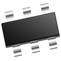
MCP4706A3T-E/CH Microchip Technology, MCP4706A3T-E/CH Datasheet - Page 65

MCP4706A3T-E/CH
Manufacturer Part Number
MCP4706A3T-E/CH
Description
Single, 8-bit NV DAC With Ext Vref And I2C Interface 6 SOT-23 T/R
Manufacturer
Microchip Technology
Series
-r
Datasheet
1.MCP4706A0T-ECH.pdf
(86 pages)
Specifications of MCP4706A3T-E/CH
Number Of Converters
1
Conversion Rate
1
Resolution
8 bit
Interface Type
I2C
Settling Time
6 us
Supply Voltage (max)
5.5 V
Supply Voltage (min)
2.7 V
Maximum Operating Temperature
+ 125 C
Mounting Style
SMD/SMT
Package / Case
SOT-23-6
Maximum Power Dissipation
452 mW
Minimum Operating Temperature
- 40 C
Supply Current
210 uA
Number Of Bits
8
Data Interface
EEPROM, I²C, Serial
Voltage Supply Source
Single Supply
Power Dissipation (max)
452mW
Operating Temperature
-40°C ~ 125°C
Mounting Type
Surface Mount
Number Of Outputs And Type
*
Lead Free Status / Rohs Status
Details
8.3
The MCP47X6 devices are rail-to-rail output DACs
designed to operate with a V
The internal output op amplifier is robust enough to
drive common, small-signal loads directly, thus
eliminating the cost and size of external buffers for
most applications. The user can use gain of 1 or 2 of
the output op amplifier by setting the configuration
register bits. Also, the user can use internal V
reference or use external reference. Various user
options and easy-to-use features make the devices
suitable for various modern DAC applications.
Application examples include:
• Decreasing Output Step Size
• Building a “Window” DAC
• Bipolar Operation
• Selectable Gain and Offset Bipolar Voltage Output
• Designing a Double-Precision DAC
• Building Programmable Current Source
• Serial Interface Communication Times
• Software I2C Interface Reset Sequence
• Power Supply Considerations
• Layout Considerations
© 2011 Microchip Technology Inc.
Application Examples
DD
range of 2.7V to 5.5V.
DD
as the
8.3.1
A
digitally-controlled set point and/or calibration of
variable parameters, such as sensor offset or slope.
For example, the MCP4726 provides 4096 output
steps. If voltage reference is 4.096V, the LSb size is
1 mV. If a smaller output step size is desired, a lower
external voltage reference is needed.
8.3.1.1
If the application is calibrating the bias voltage of a
diode or transistor, a bias voltage range of 0.8V may be
desired with about 200 µV resolution per step. Two
common methods to achieve small step size are using
lower V
DAC’s output.
Using an external voltage reference (V
option, if the external reference is available with the
desired output voltage range. However, occasionally,
when using a low-voltage reference voltage, the noise
floor causes a SNR error that is intolerable. Using a
voltage divider method is another option, and provides
some advantages when external voltage reference
needs to be very low, or when the desired output
voltage is not available. In this case, a larger value
reference voltage is used, while two resistors scale the
output range down to the precise desired level.
Figure 8-3
on the output of the voltage divider plays a critical
function in attenuating the output noise of the DAC and
the induced noise from the environment.
FIGURE 8-3:
or Threshold Calibration.
EQUATION 8-1:
2-wire
I
Optional
2
MCP4706/4716/4726
V
C™
V
V trip
MCP47X6
common
OUT
REF
REF
= V
V
=
illustrates this concept. A bypass capacitor
DD
pin voltage or using a voltage divider on the
DC SET POINT OR CALIBRATION
REF
V OUT
Decreasing Output Step Size
application
R
V
• G •
SENSE
O
⎛
⎜
⎝
--------------------
R 1
R
1
R 2
V
Example Circuit Of Set Point
V
CALCULATIONS
+
DAC Register Value
R
DD
OUT
R 2
2
⎞
⎟
⎠
for
AND V
2
N
the
C
V
1
TRIP
DS22272A-page 65
TRIP
devices
Comp.
V
REF
V
CC
CC
) is an
+
–
V
is
OUT
a


