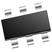
MCP4706A3T-E/CH Microchip Technology, MCP4706A3T-E/CH Datasheet - Page 51

MCP4706A3T-E/CH
Manufacturer Part Number
MCP4706A3T-E/CH
Description
Single, 8-bit NV DAC With Ext Vref And I2C Interface 6 SOT-23 T/R
Manufacturer
Microchip Technology
Series
-r
Datasheet
1.MCP4706A0T-ECH.pdf
(86 pages)
Specifications of MCP4706A3T-E/CH
Number Of Converters
1
Conversion Rate
1
Resolution
8 bit
Interface Type
I2C
Settling Time
6 us
Supply Voltage (max)
5.5 V
Supply Voltage (min)
2.7 V
Maximum Operating Temperature
+ 125 C
Mounting Style
SMD/SMT
Package / Case
SOT-23-6
Maximum Power Dissipation
452 mW
Minimum Operating Temperature
- 40 C
Supply Current
210 uA
Number Of Bits
8
Data Interface
EEPROM, I²C, Serial
Voltage Supply Source
Single Supply
Power Dissipation (max)
452mW
Operating Temperature
-40°C ~ 125°C
Mounting Type
Surface Mount
Number Of Outputs And Type
*
Lead Free Status / Rohs Status
Details
6.2
This write command is used to update the volatile DAC
Register value and configuration bits. The EEPROM is
not affected by this command.
example of this write command.
The volatile DAC register and configuration bits are
updated with the written date at the completion of the
ACK bit (falling edge of SCL).
FIGURE 6-2:
© 2011 Microchip Technology Inc.
Note 1:
SDA
SCL
Legend:
3:
2:
Write Volatile Memory
(C2:C0 = ‘010’)
S
Start bit
The device updates V
The 2nd - 4th bytes can be repeated after the 4th byte by continued clocking before issuing Stop bit.
ACK bit generated by MCP47X6.
1
D09:D00 = 10-bit data for MCP4716 device
D07:D00 = 8-bit data for MCP4706 device
D11:D00 = 12-bit data for MCP4726 device
X = don’t care
MCP4726
MCP4716
MCP4706
Device Addressing
1
0
Write Volatile Memory Command.
0
D11 D10 D09 D08 D07 D06 D05 D04 D03 D02 D01 D00
D09 D08 D07 D06 D05 D04 D03 D02 D01 D00
D07 D06 D05 D04 D03 D02 D01 D00
b15 b14 b13 b12 b11 b10 b09 b08 b07 b06 b05 b04 b03 b02 b01 b00
A2 A1 A0
OUT
Figure 6-2
at the falling edge of the SCL at the end of this ACK pulse.
R/W
Read/Write bit (Write)
0
A
ACK bit
0
shows an
Command
bits
0
Data bits (16 bits) (3rd + 4th bytes)
(3)
1
0
VREF1
Ref.
Voltage
Select
bits
VREF0
PD1 PD0
Power
Down
bits
After this ACK bit, the I
Stop bit or the I
command bits + 5 configuration bits), and the 3rd byte
(8 data bits (b15:b08)), and the 4th byte (8 data bits
(b07:b00)). Repeating the 2nd through 4th bytes allows
a continuous command where the volatile DAC register
and configuration bits can be updated without the
communication overhead of the device addressing
byte (1st byte).
MCP4706/4716/4726
X
Gain
bit
X
G
ACK bit
A
0
X
X
b15 b14 b13 b12 b11 b10 b09 b08
b07 b06 b05 b04 b03 b02 b01 b00
X
X
Data bits (8 bits) (3rd byte)
Data bits (8 bits) (4th byte)
2
(3)
C Master can repeat the 2nd (3
X
X
X
2
C Master should generate a
X
X
X
X
X
X
ACK bit
ACK bit
X
X
X
DS22272A-page 51
(3)
(3)
Note 1
Note 2
A
A
Stop bit
0
0
P


