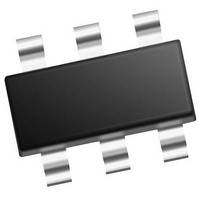
MCP4706A3T-E/CH Microchip Technology, MCP4706A3T-E/CH Datasheet - Page 47

MCP4706A3T-E/CH
Manufacturer Part Number
MCP4706A3T-E/CH
Description
Single, 8-bit NV DAC With Ext Vref And I2C Interface 6 SOT-23 T/R
Manufacturer
Microchip Technology
Series
-r
Datasheet
1.MCP4706A0T-ECH.pdf
(86 pages)
Specifications of MCP4706A3T-E/CH
Number Of Converters
1
Conversion Rate
1
Resolution
8 bit
Interface Type
I2C
Settling Time
6 us
Supply Voltage (max)
5.5 V
Supply Voltage (min)
2.7 V
Maximum Operating Temperature
+ 125 C
Mounting Style
SMD/SMT
Package / Case
SOT-23-6
Maximum Power Dissipation
452 mW
Minimum Operating Temperature
- 40 C
Supply Current
210 uA
Number Of Bits
8
Data Interface
EEPROM, I²C, Serial
Voltage Supply Source
Single Supply
Power Dissipation (max)
452mW
Operating Temperature
-40°C ~ 125°C
Mounting Type
Surface Mount
Number Of Outputs And Type
*
Lead Free Status / Rohs Status
Details
5.3.6
The I
device must be ‘activated’ to operate in high-speed
(3.4 Mbit/s) mode. This is done by the Master sending
a special address byte following the START bit. This
byte is referred to as the high-speed Master Mode
Code (HSMMC).
The MCP47X6 device does not acknowledge this byte.
However, upon receiving this command, the device
switches to HS mode. The device can now
communicate at up to 3.4 Mbit/s on SDA and SCL
lines. The device will switch out of the HS mode on the
next STOP condition.
The master code is sent as follows:
1.
2.
3.
FIGURE 5-10:
© 2011 Microchip Technology Inc.
S
START condition (S)
High-Speed Master Mode Code (0000 1XXX),
The XXX bits are unique to the high-speed (HS)
mode Master.
No Acknowledge (A)
2
R/W = Read/Write bit
C specification requires that a high-speed mode
F/S-mode
‘0 0 0 0 1 X X X’b
Sr = Repeated Start bit
S = Start bit
A = Acknowledge bit
A = Not Acknowledge bit
P = Stop bit (Stop condition terminates HS Mode)
HS Select Byte
HS MODE
HS Mode Sequence.
A
Sr
HS-mode
‘Slave Address’
Control Byte
R/W
A
Command/Data Byte(s)
After switching to the High-Speed mode, the next
transferred byte is the I
the device to communicate with, and any number of
data bytes plus acknowledgements. The Master
Device can then either issue a Repeated Start bit to
address a different device (at High-Speed) or a Stop bit
to return to Fast/Standard bus speed. After the Stop bit,
any other Master Device (in a Multi-Master system) can
arbitrate for the I
See
sequence.
For more information on the HS mode, or other I
modes, please refer to the NXP I
5.3.6.1
The slope control on the SDA output is different
between the Fast/Standard Speed and the High-Speed
clock modes of the interface.
5.3.6.2
The pulse gobbler on the SCL pin is automatically
adjusted to suppress spikes < 10 ns during HS mode.
“Data”
MCP4706/4716/4726
Figure 5-10
Slope Control
Pulse Gobbler
A/A
2
for illustration of HS mode command
C bus.
Sr
P
‘Slave Address’ R/W
HS-mode continues
2
C control byte, which specifies
Control Byte
F/S-mode
2
C specification.
DS22272A-page 47
A
2
C


