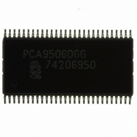
PCA9506DGG,512 NXP Semiconductors, PCA9506DGG,512 Datasheet - Page 11

PCA9506DGG,512
Manufacturer Part Number
PCA9506DGG,512
Description
IC I/O EXPANDER I2C 40B 56TSSOP
Manufacturer
NXP Semiconductors
Datasheet
1.PCA9505DGG112.pdf
(34 pages)
Specifications of PCA9506DGG,512
Package / Case
56-TSSOP
Interface
I²C
Number Of I /o
40
Interrupt Output
Yes
Frequency - Clock
400kHz
Voltage - Supply
2.3 V ~ 5.5 V
Operating Temperature
-40°C ~ 85°C
Mounting Type
Surface Mount
Includes
POR
Logic Family
PCA9506
Number Of Lines (input / Output)
40.0 / 40.0
Operating Supply Voltage
2.3 V to 5.5 V
Power Dissipation
500 mW
Operating Temperature Range
- 40 C to + 85 C
Input Voltage
5.5 V
Logic Type
I/O Expander
Maximum Clock Frequency
400 KHz
Mounting Style
SMD/SMT
Number Of Input Lines
40.0
Number Of Output Lines
40.0
Output Current
50 mA
Output Voltage
5.5 V
Lead Free Status / RoHS Status
Lead free / RoHS Compliant
Lead Free Status / RoHS Status
Lead free / RoHS Compliant, Lead free / RoHS Compliant
Other names
568-3354-5
935280798512
PCA9506DGG
935280798512
PCA9506DGG
Available stocks
Company
Part Number
Manufacturer
Quantity
Price
Part Number:
PCA9506DGG,512
Manufacturer:
NXP/恩智浦
Quantity:
20 000
NXP Semiconductors
Table 5.
Legend: * default value.
Table 6.
Legend: * default value.
PCA9505_9506
Product data sheet
Address
08h
09h
0Ah
0Bh
0Ch
Address
10h
11h
12h
13h
14h
OP0 to OP4 - Output Port registers (address 08h to 0Ch) bit description
PI0 to PI4 - Polarity Inversion registers (address 10h to 14h) bit description
Register
OP0
OP1
OP2
OP3
OP4
Register
PI0
PI1
PI2
PI3
PI4
7.3.2 OP0 to OP4 - Output Port registers
7.3.3 PI0 to PI4 - Polarity Inversion registers
These registers reflect the outgoing logic levels of the pins defined as outputs by the
I/O Configuration register. Bit values in these registers have no effect on pins defined as
inputs. In turn, reads from these registers reflect the values that are in the flip-flops
controlling the output selection, not the actual pin values.
Where ‘x’ refers to the bank number (0 to 4); ‘y’ refers to the bit number (0 to 7).
These registers allow inversion of the polarity of the corresponding Input Port register.
Where ‘x’ refers to the bank number (0 to 4); ‘y’ refers to the bit number (0 to 7).
Ox[y] = 0: IOx_y = 0 if IOx_y defined as output (Cx[y] in IOC register = 0).
Ox[y] = 1: IOx_y = 1 if IOx_y defined as output (Cx[y] in IOC register = 0).
Px[y] = 0: The corresponding Input Port register data polarity is retained.
Px[y] = 1: The corresponding Input Port register data polarity is inverted.
Bit
7 to 0
7 to 0
7 to 0
7 to 0
7 to 0
Bit
7 to 0
7 to 0
7 to 0
7 to 0
7 to 0
All information provided in this document is subject to legal disclaimers.
Symbol
O0[7:0]
O1[7:0]
O2[7:0]
O3[7:0]
O4[7:0]
Symbol
P0[7:0]
P1[7:0]
P2[7:0]
P3[7:0]
P4[7:0]
Rev. 4 — 3 August 2010
Access
R/W
R/W
R/W
R/W
R/W
Access
R/W
R/W
R/W
R/W
R/W
40-bit I
0000 0000*
0000 0000*
0000 0000*
0000 0000*
0000 0000*
Value
Value
0000 0000*
0000 0000*
0000 0000*
0000 0000*
0000 0000*
2
C-bus I/O port with RESET, OE and INT
Description
Output Port register bank 0
Output Port register bank 1
Output Port register bank 2
Output Port register bank 3
Output Port register bank 4
Description
Polarity Inversion register bank 0
Polarity Inversion register bank 1
Polarity Inversion register bank 2
Polarity Inversion register bank 3
Polarity Inversion register bank 4
PCA9505/06
© NXP B.V. 2010. All rights reserved.
11 of 34


