PCA9506DGG,512 NXP Semiconductors, PCA9506DGG,512 Datasheet - Page 8
PCA9506DGG,512
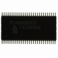
Manufacturer Part Number
PCA9506DGG,512
Description
IC I/O EXPANDER I2C 40B 56TSSOP
Manufacturer
NXP Semiconductors
Datasheet
1.PCA9505DGG112.pdf
(34 pages)
Specifications of PCA9506DGG,512
Package / Case
56-TSSOP
Interface
I²C
Number Of I /o
40
Interrupt Output
Yes
Frequency - Clock
400kHz
Voltage - Supply
2.3 V ~ 5.5 V
Operating Temperature
-40°C ~ 85°C
Mounting Type
Surface Mount
Includes
POR
Logic Family
PCA9506
Number Of Lines (input / Output)
40.0 / 40.0
Operating Supply Voltage
2.3 V to 5.5 V
Power Dissipation
500 mW
Operating Temperature Range
- 40 C to + 85 C
Input Voltage
5.5 V
Logic Type
I/O Expander
Maximum Clock Frequency
400 KHz
Mounting Style
SMD/SMT
Number Of Input Lines
40.0
Number Of Output Lines
40.0
Output Current
50 mA
Output Voltage
5.5 V
Lead Free Status / RoHS Status
Lead free / RoHS Compliant
Lead Free Status / RoHS Status
Lead free / RoHS Compliant, Lead free / RoHS Compliant
Other names
568-3354-5
935280798512
PCA9506DGG
935280798512
PCA9506DGG
Available stocks
Company
Part Number
Manufacturer
Quantity
Price

Part Number:
PCA9506DGG,512
Manufacturer:
NXP/恩智浦
Quantity:
20 000


NXP Semiconductors
PCA9505_9506
Product data sheet
The lowest 6 bits are used as a pointer to determine which register will be accessed. The
registers are:
If the Auto-Increment flag is set (AI = 1), the 3 least significant bits are automatically
incremented after a read or write. This allows the user to program and/or read the
5 register banks sequentially.
If more than 5 bytes of data are written and AI = 1, previous data in the selected registers
will be overwritten. Reserved registers are skipped and not accessed (refer to
If the Auto-Increment flag is cleared (AI = 0), the 3 least significant bits are not
incremented after data is read or written. During a read operation, the same register bank
is read each time. During a write operation, data is written to the same register bank each
time.
Only a Command register code with the 5 least significant bits equal to the 25 allowable
values as defined in
be accessed for proper device functionality. At power-up, this register defaults to 0x80,
with the AI bit set to logic 1, and the lowest 7 bits set to logic 0.
During a write operation, the PCA9505/06 will acknowledge a byte sent to OPx, PIx, and
IOCx and MSKx registers, but will not acknowledge a byte sent to the IPx registers since
these are read-only registers.
•
•
•
•
•
IP: Input Port registers (5 registers)
OP: Output Port registers (5 registers)
PI: Polarity Inversion registers (5 registers)
IOC: I/O Configuration registers (5 registers)
MSK: Mask interrupt registers (5 registers)
All information provided in this document is subject to legal disclaimers.
Table 3
Rev. 4 — 3 August 2010
are valid. Reserved or undefined command codes must not
40-bit I
2
C-bus I/O port with RESET, OE and INT
PCA9505/06
© NXP B.V. 2010. All rights reserved.
Table
8 of 34
3).
Related parts for PCA9506DGG,512
Image
Part Number
Description
Manufacturer
Datasheet
Request
R

Part Number:
Description:
NXP Semiconductors designed the LPC2420/2460 microcontroller around a 16-bit/32-bitARM7TDMI-S CPU core with real-time debug interfaces that include both JTAG andembedded trace
Manufacturer:
NXP Semiconductors
Datasheet:

Part Number:
Description:
NXP Semiconductors designed the LPC2458 microcontroller around a 16-bit/32-bitARM7TDMI-S CPU core with real-time debug interfaces that include both JTAG andembedded trace
Manufacturer:
NXP Semiconductors
Datasheet:
Part Number:
Description:
NXP Semiconductors designed the LPC2468 microcontroller around a 16-bit/32-bitARM7TDMI-S CPU core with real-time debug interfaces that include both JTAG andembedded trace
Manufacturer:
NXP Semiconductors
Datasheet:
Part Number:
Description:
NXP Semiconductors designed the LPC2470 microcontroller, powered by theARM7TDMI-S core, to be a highly integrated microcontroller for a wide range ofapplications that require advanced communications and high quality graphic displays
Manufacturer:
NXP Semiconductors
Datasheet:
Part Number:
Description:
NXP Semiconductors designed the LPC2478 microcontroller, powered by theARM7TDMI-S core, to be a highly integrated microcontroller for a wide range ofapplications that require advanced communications and high quality graphic displays
Manufacturer:
NXP Semiconductors
Datasheet:
Part Number:
Description:
The Philips Semiconductors XA (eXtended Architecture) family of 16-bit single-chip microcontrollers is powerful enough to easily handle the requirements of high performance embedded applications, yet inexpensive enough to compete in the market for hi
Manufacturer:
NXP Semiconductors
Datasheet:
Part Number:
Description:
The XA-S3 device is a member of Philips Semiconductors? XA(eXtended Architecture) family of high performance 16-bitsingle-chip microcontrollers
Manufacturer:
NXP Semiconductors
Datasheet:

Part Number:
Description:
The NXP BlueStreak LH75401/LH75411 family consists of two low-cost 16/32-bit System-on-Chip (SoC) devices
Manufacturer:
NXP Semiconductors
Datasheet:
Part Number:
Description:
The NXP LPC3130/3131 combine an 180 MHz ARM926EJ-S CPU core, high-speed USB2
Manufacturer:
NXP Semiconductors
Datasheet:
Part Number:
Description:
The NXP LPC3141 combine a 270 MHz ARM926EJ-S CPU core, High-speed USB 2
Manufacturer:
NXP Semiconductors
Part Number:
Description:
The NXP LPC3143 combine a 270 MHz ARM926EJ-S CPU core, High-speed USB 2
Manufacturer:
NXP Semiconductors

Part Number:
Description:
The NXP LPC3152 combines an 180 MHz ARM926EJ-S CPU core, High-speed USB 2
Manufacturer:
NXP Semiconductors
Part Number:
Description:
The NXP LPC3154 combines an 180 MHz ARM926EJ-S CPU core, High-speed USB 2
Manufacturer:
NXP Semiconductors

Part Number:
Description:
Standard level N-channel enhancement mode Field-Effect Transistor (FET) in a plastic package using NXP High-Performance Automotive (HPA) TrenchMOS technology
Manufacturer:
NXP Semiconductors
Datasheet: