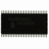
PCA9506DGG,512 NXP Semiconductors, PCA9506DGG,512 Datasheet - Page 17

PCA9506DGG,512
Manufacturer Part Number
PCA9506DGG,512
Description
IC I/O EXPANDER I2C 40B 56TSSOP
Manufacturer
NXP Semiconductors
Datasheet
1.PCA9505DGG112.pdf
(34 pages)
Specifications of PCA9506DGG,512
Package / Case
56-TSSOP
Interface
I²C
Number Of I /o
40
Interrupt Output
Yes
Frequency - Clock
400kHz
Voltage - Supply
2.3 V ~ 5.5 V
Operating Temperature
-40°C ~ 85°C
Mounting Type
Surface Mount
Includes
POR
Logic Family
PCA9506
Number Of Lines (input / Output)
40.0 / 40.0
Operating Supply Voltage
2.3 V to 5.5 V
Power Dissipation
500 mW
Operating Temperature Range
- 40 C to + 85 C
Input Voltage
5.5 V
Logic Type
I/O Expander
Maximum Clock Frequency
400 KHz
Mounting Style
SMD/SMT
Number Of Input Lines
40.0
Number Of Output Lines
40.0
Output Current
50 mA
Output Voltage
5.5 V
Lead Free Status / RoHS Status
Lead free / RoHS Compliant
Lead Free Status / RoHS Status
Lead free / RoHS Compliant, Lead free / RoHS Compliant
Other names
568-3354-5
935280798512
PCA9506DGG
935280798512
PCA9506DGG
Available stocks
Company
Part Number
Manufacturer
Quantity
Price
Part Number:
PCA9506DGG,512
Manufacturer:
NXP/恩智浦
Quantity:
20 000
Fig 12. Write to a specific output port
Fig 13. Write to the I/O Configuration, Polarity Inversion or Mask Interrupt registers
SDA
OE is LOW to observe a change in the outputs.
Two, three, or four adjacent banks can be programmed by using the Auto-Increment feature (AI = 1) and change at the corresponding output port becomes effective at
each acknowledge.
The programming becomes effective at the acknowledge.
Less than 5 bytes can be programmed by using this scheme. D5, D4, D3, D2, D1, D0 refers to the first register to be programmed.
If more than 5 bytes are written, previous data are overwritten (the sixth Configuration register will roll over to the first addressed Configuration register, the sixth Polarity
Inversion register will roll over to the first addressed Polarity Inversion register and the sixth Mask Interrupt register will roll over to the first addressed Mask Interrupt
register).
S
START condition
0 1 0 0 A2 A1 A0 0
slave address
acknowledge
from slave
SDA
write to port
data out from port
R/W
S
START condition
A
0 1 0 0 A2 A1 A0 0
AI = 1
1 0 D5 D4 D3 D2 D1 D0
command register
slave address
acknowledge
from slave
D[5:0] = 01 0000 for Polarity Inversion register programming bank 0
D[5:0] = 01 1000 for Configuration register programming bank 0
D[5:0] = 10 0000 for Mask Interrupt register programming bank 0
R/W
A
A
acknowledge
from slave
AI 0 0 0 1 D2 D1 D0 A
DATA BANK 0
acknowledge
A
acknowledge
from slave
from slave
DATA BANK 1
DATA BANK X
A
acknowledge
from slave
DATA BANK 2
acknowledge
from slave
A
A
t
v(Q)
P
STOP
condition
A
acknowledge
from slave
DATA BANK 3
002aab497
data X
valid
acknowledge
from slave
A
DATA BANK 4
acknowledge
from slave
condition
002aab498
STOP
A
P


