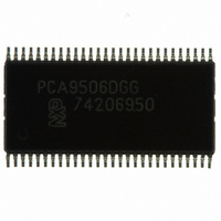
PCA9506DGG,512 NXP Semiconductors, PCA9506DGG,512 Datasheet - Page 15

PCA9506DGG,512
Manufacturer Part Number
PCA9506DGG,512
Description
IC I/O EXPANDER I2C 40B 56TSSOP
Manufacturer
NXP Semiconductors
Datasheet
1.PCA9505DGG112.pdf
(34 pages)
Specifications of PCA9506DGG,512
Package / Case
56-TSSOP
Interface
I²C
Number Of I /o
40
Interrupt Output
Yes
Frequency - Clock
400kHz
Voltage - Supply
2.3 V ~ 5.5 V
Operating Temperature
-40°C ~ 85°C
Mounting Type
Surface Mount
Includes
POR
Logic Family
PCA9506
Number Of Lines (input / Output)
40.0 / 40.0
Operating Supply Voltage
2.3 V to 5.5 V
Power Dissipation
500 mW
Operating Temperature Range
- 40 C to + 85 C
Input Voltage
5.5 V
Logic Type
I/O Expander
Maximum Clock Frequency
400 KHz
Mounting Style
SMD/SMT
Number Of Input Lines
40.0
Number Of Output Lines
40.0
Output Current
50 mA
Output Voltage
5.5 V
Lead Free Status / RoHS Status
Lead free / RoHS Compliant
Lead Free Status / RoHS Status
Lead free / RoHS Compliant, Lead free / RoHS Compliant
Other names
568-3354-5
935280798512
PCA9506DGG
935280798512
PCA9506DGG
Available stocks
Company
Part Number
Manufacturer
Quantity
Price
Part Number:
PCA9506DGG,512
Manufacturer:
NXP/恩智浦
Quantity:
20 000
NXP Semiconductors
PCA9505_9506
Product data sheet
Fig 9.
SDA
SCL
System configuration
TRANSMITTER/
RECEIVER
MASTER
8.3 Acknowledge
8.4 Bus transactions
The number of data bytes transferred between the START and the STOP conditions from
transmitter to receiver is not limited. Each byte of eight bits is followed by one
acknowledge bit. The acknowledge bit is a HIGH level put on the bus by the transmitter,
whereas the master generates an extra acknowledge related clock pulse.
A slave receiver which is addressed must generate an acknowledge after the reception of
each byte. Also a master must generate an acknowledge after the reception of each byte
that has been clocked out of the slave transmitter. The device that acknowledges has to
pull down the SDA line during the acknowledge clock pulse, so that the SDA line is stable
LOW during the HIGH period of the acknowledge related clock pulse; set-up and hold
times must be taken into account.
A master receiver must signal an end of data to the transmitter by not generating an
acknowledge on the last byte that has been clocked out of the slave. In this event, the
transmitter must leave the data line HIGH to enable the master to generate a STOP
condition.
Data is transmitted to the PCA9505/06 registers using Write Byte transfers (see
Figure
Receive Byte transfers (see
Fig 10. Acknowledgement on the I
12, and
RECEIVER
SLAVE
SCL from master
by transmitter
data output
Figure
data output
by receiver
All information provided in this document is subject to legal disclaimers.
TRANSMITTER/
13). Data is read from the PCA9505/06 registers using Read and
Rev. 4 — 3 August 2010
RECEIVER
condition
START
SLAVE
S
Figure
2
14).
C-bus
TRANSMITTER
1
40-bit I
MASTER
2
2
C-bus I/O port with RESET, OE and INT
TRANSMITTER/
RECEIVER
MASTER
acknowledgement
not acknowledge
SLAVE
clock pulse for
acknowledge
8
PCA9505/06
MULTIPLEXER
© NXP B.V. 2010. All rights reserved.
002aaa987
I
2
9
C-BUS
002aaa966
Figure
15 of 34
11,


