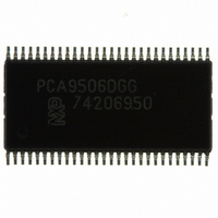
PCA9506DGG,512 NXP Semiconductors, PCA9506DGG,512 Datasheet - Page 23

PCA9506DGG,512
Manufacturer Part Number
PCA9506DGG,512
Description
IC I/O EXPANDER I2C 40B 56TSSOP
Manufacturer
NXP Semiconductors
Datasheet
1.PCA9505DGG112.pdf
(34 pages)
Specifications of PCA9506DGG,512
Package / Case
56-TSSOP
Interface
I²C
Number Of I /o
40
Interrupt Output
Yes
Frequency - Clock
400kHz
Voltage - Supply
2.3 V ~ 5.5 V
Operating Temperature
-40°C ~ 85°C
Mounting Type
Surface Mount
Includes
POR
Logic Family
PCA9506
Number Of Lines (input / Output)
40.0 / 40.0
Operating Supply Voltage
2.3 V to 5.5 V
Power Dissipation
500 mW
Operating Temperature Range
- 40 C to + 85 C
Input Voltage
5.5 V
Logic Type
I/O Expander
Maximum Clock Frequency
400 KHz
Mounting Style
SMD/SMT
Number Of Input Lines
40.0
Number Of Output Lines
40.0
Output Current
50 mA
Output Voltage
5.5 V
Lead Free Status / RoHS Status
Lead free / RoHS Compliant
Lead Free Status / RoHS Status
Lead free / RoHS Compliant, Lead free / RoHS Compliant
Other names
568-3354-5
935280798512
PCA9506DGG
935280798512
PCA9506DGG
Available stocks
Company
Part Number
Manufacturer
Quantity
Price
Part Number:
PCA9506DGG,512
Manufacturer:
NXP/恩智浦
Quantity:
20 000
NXP Semiconductors
Table 11.
[1]
[2]
[3]
[4]
[5]
[6]
[7]
PCA9505_9506
Product data sheet
Symbol
Reset
t
t
t
w(rst)
rec(rst)
rst
Fig 16. Definition of timing on the I
Minimum SCL clock frequency is limited by the bus time-out feature, which resets the serial bus interface if either SDA or SCL is held
LOW for a minimum of 25 ms. Disable bus time-out feature for DC operation.
t
t
A master device must internally provide a hold time of at least 300 ns for the SDA signal (refer to the V
bridge the undefined region SCL’s falling edge.
The maximum t
250 ns. This allows series protection resistors to be connected between the SDA and the SCL pins and the SDA/SCL bus lines without
exceeding the maximum specified t
C
Input filters on the SDA and SCL inputs suppress noise spikes less than 50 ns.
VD;ACK
VD;DAT
b
SDA
SCL
= total capacitance of one bus line in pF.
= minimum time for SDA data out to be valid following SCL LOW.
= time for Acknowledgement signal from SCL LOW to SDA (out) LOW.
Parameter
reset pulse width
reset recovery time
reset time
Dynamic characteristics
P
t
BUF
f
for the SDA and SCL bus lines is specified at 300 ns. The maximum fall time for the SDA output stage t
S
t
HD;STA
t
LOW
f
.
…continued
2
t
t
r
HD;DAT
C-bus
All information provided in this document is subject to legal disclaimers.
Conditions
Rev. 4 — 3 August 2010
t
HIGH
t
f
t
SU;DAT
40-bit I
Standard mode
Min
100
4
0
I
2
2
C-bus
C-bus I/O port with RESET, OE and INT
Sr
Max
t
SU;STA
-
-
-
t
HD;STA
Fast mode I
IL
PCA9505/06
Min
100
of the SCL signal) in order to
4
0
t
SP
t
SU;STO
© NXP B.V. 2010. All rights reserved.
2
C-bus
Max
002aaa986
f
-
-
-
is specified at
P
23 of 34
Unit
ns
ns
ns


