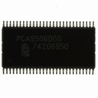
PCA9506DGG,512 NXP Semiconductors, PCA9506DGG,512 Datasheet - Page 7

PCA9506DGG,512
Manufacturer Part Number
PCA9506DGG,512
Description
IC I/O EXPANDER I2C 40B 56TSSOP
Manufacturer
NXP Semiconductors
Datasheet
1.PCA9505DGG112.pdf
(34 pages)
Specifications of PCA9506DGG,512
Package / Case
56-TSSOP
Interface
I²C
Number Of I /o
40
Interrupt Output
Yes
Frequency - Clock
400kHz
Voltage - Supply
2.3 V ~ 5.5 V
Operating Temperature
-40°C ~ 85°C
Mounting Type
Surface Mount
Includes
POR
Logic Family
PCA9506
Number Of Lines (input / Output)
40.0 / 40.0
Operating Supply Voltage
2.3 V to 5.5 V
Power Dissipation
500 mW
Operating Temperature Range
- 40 C to + 85 C
Input Voltage
5.5 V
Logic Type
I/O Expander
Maximum Clock Frequency
400 KHz
Mounting Style
SMD/SMT
Number Of Input Lines
40.0
Number Of Output Lines
40.0
Output Current
50 mA
Output Voltage
5.5 V
Lead Free Status / RoHS Status
Lead free / RoHS Compliant
Lead Free Status / RoHS Status
Lead free / RoHS Compliant, Lead free / RoHS Compliant
Other names
568-3354-5
935280798512
PCA9506DGG
935280798512
PCA9506DGG
Available stocks
Company
Part Number
Manufacturer
Quantity
Price
Part Number:
PCA9506DGG,512
Manufacturer:
NXP/恩智浦
Quantity:
20 000
NXP Semiconductors
7. Functional description
PCA9505_9506
Product data sheet
7.1 Device address
7.2 Command register
Table 2.
[1]
Refer to
IO0_0 to
Following a START condition, the bus master must send the address of the slave it is
accessing and the operation it wants to perform (read or write). The address of the
PCA9505/06 is shown in
addresses and need to be connected to V
pull-up resistors are incorporated on A2, A1, and A0.
The last bit of the first byte defines the operation to be performed. When set to logic 1 a
read is selected, while a logic 0 selects a write operation.
Following the successful acknowledgement of the slave address + R/W bit, the bus
master will send a byte to the PCA9505/06, which will be stored in the Command register.
Symbol
OE
INT
RESET
Fig 5.
Fig 6.
HVQFN56 package die supply ground is connected to both V
must be connected to supply ground for proper device operation. For enhanced thermal, electrical, and
board level performance, the exposed pad needs to be soldered to the board using a corresponding
thermal pad on the board and for proper heat conduction through the board, thermal vias need to be
incorporated in the printed-circuit board in the thermal pad region.
Figure 1 “Block diagram of PCA9505/06”
IO4_7”.
PCA9505/06 address
Command register
Pin description
All information provided in this document is subject to legal disclaimers.
Pin
TSSOP56
30
55
56
Rev. 4 — 3 August 2010
AI
Auto-Increment
1
Figure
…continued
−
0
0
D5
0
5. Slave address pins A2, A1, and A0 choose 1 of 8 slave
HVQFN56
23
48
49
1
D4
fixed
0
register number
slave address
0
D3
0
40-bit I
DD
0
D2
0
(1) or V
programmable
A2
002aab495
D1
2
0
C-bus I/O port with RESET, OE and INT
A1
and
D0
Type
I
O
I
0
SS
SS
002aab494
A0 R/W
default at power-up
or after RESET
Figure 2 “Simplified schematic of
(0). To conserve power, no internal
pins and exposed center pad. V
Description
active LOW output enable input
active LOW interrupt output
active LOW reset input
PCA9505/06
© NXP B.V. 2010. All rights reserved.
SS
pins
7 of 34


