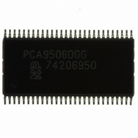
PCA9506DGG,512 NXP Semiconductors, PCA9506DGG,512 Datasheet - Page 12

PCA9506DGG,512
Manufacturer Part Number
PCA9506DGG,512
Description
IC I/O EXPANDER I2C 40B 56TSSOP
Manufacturer
NXP Semiconductors
Datasheet
1.PCA9505DGG112.pdf
(34 pages)
Specifications of PCA9506DGG,512
Package / Case
56-TSSOP
Interface
I²C
Number Of I /o
40
Interrupt Output
Yes
Frequency - Clock
400kHz
Voltage - Supply
2.3 V ~ 5.5 V
Operating Temperature
-40°C ~ 85°C
Mounting Type
Surface Mount
Includes
POR
Logic Family
PCA9506
Number Of Lines (input / Output)
40.0 / 40.0
Operating Supply Voltage
2.3 V to 5.5 V
Power Dissipation
500 mW
Operating Temperature Range
- 40 C to + 85 C
Input Voltage
5.5 V
Logic Type
I/O Expander
Maximum Clock Frequency
400 KHz
Mounting Style
SMD/SMT
Number Of Input Lines
40.0
Number Of Output Lines
40.0
Output Current
50 mA
Output Voltage
5.5 V
Lead Free Status / RoHS Status
Lead free / RoHS Compliant
Lead Free Status / RoHS Status
Lead free / RoHS Compliant, Lead free / RoHS Compliant
Other names
568-3354-5
935280798512
PCA9506DGG
935280798512
PCA9506DGG
Available stocks
Company
Part Number
Manufacturer
Quantity
Price
Part Number:
PCA9506DGG,512
Manufacturer:
NXP/恩智浦
Quantity:
20 000
NXP Semiconductors
Table 7.
Legend: * default value.
Table 8.
Legend: * default value.
PCA9505_9506
Product data sheet
Address
18h
19h
1Ah
1Bh
1Ch
Address
20h
21h
22h
23h
24h
IOC0 to IOC4 - I/O Configuration registers (address 18h to 1Ch) bit description
MSK0 to MSK4 - Mask interrupt registers (address 20h to 24h) bit description
Register
IOC0
IOC1
IOC2
IOC3
IOC4
Register
MSK0
MSK1
MSK2
MSK3
MSK4
7.3.4 IOC0 to IOC4 - I/O Configuration registers
7.3.5 MSK0 to MSK4 - Mask interrupt registers
7.4 Power-on reset
7.5 RESET input
These registers configure the direction of the I/O pins.
Where ‘x’ refers to the bank number (0 to 4); ‘y’ refers to the bit number (0 to 7).
These registers mask the interrupt due to a change in the I/O pins configured as inputs.
‘x’ refers to the bank number (0 to 4); ‘y’ refers to the bit number (0 to 7).
When power is applied to V
in a reset condition until V
released and the PCA9505/06 registers and I
default states. Thereafter, V
A reset can be accomplished by holding the RESET pin LOW for a minimum of t
PCA9505/06 registers and I
the RESET input is once again HIGH.
Cx[y] = 0: The corresponding port pin is an output.
Cx[y] = 1: The corresponding port pin is an input.
Mx[y] = 0: A level change at the I/O will generate an interrupt if IOx_y defined as input
(Cx[y] in IOC register = 1).
Mx[y] = 1: A level change in the input port will not generate an interrupt if IOx_y defined
as input (Cx[y] in IOC register = 1).
Bit
7 to 0
7 to 0
7 to 0
7 to 0
7 to 0
Bit
7 to 0
7 to 0
7 to 0
7 to 0
7 to 0
All information provided in this document is subject to legal disclaimers.
Symbol
C0[7:0]
C1[7:0]
C2[7:0]
C3[7:0]
C4[7:0]
Symbol
M0[7:0]
M1[7:0]
M2[7:0]
M3[7:0]
M4[7:0]
Rev. 4 — 3 August 2010
DD
DD
DD
2
C-bus state machine will be held in their default states until
has reached V
, an internal Power-On Reset (POR) holds the PCA9505/06
Access
R/W
R/W
R/W
R/W
R/W
Access
R/W
R/W
R/W
R/W
R/W
must be lowered below 0.2 V to reset the device.
40-bit I
Value
1111 1111*
1111 1111*
1111 1111*
1111 1111*
1111 1111*
Value
1111 1111*
1111 1111*
1111 1111*
1111 1111*
1111 1111*
POR
2
C-bus state machine will initialize to their
2
. At that point, the reset condition is
C-bus I/O port with RESET, OE and INT
Mask Interrupt register bank 0
Mask Interrupt register bank 1
Mask Interrupt register bank 2
Mask Interrupt register bank 3
Mask Interrupt register bank 4
Description
I/O Configuration register bank 0
I/O Configuration register bank 1
I/O Configuration register bank 2
I/O Configuration register bank 3
I/O Configuration register bank 4
Description
PCA9505/06
© NXP B.V. 2010. All rights reserved.
w(rst)
12 of 34
. The


