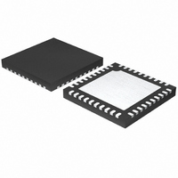
ISL6334ACRZ Intersil, ISL6334ACRZ Datasheet - Page 12

ISL6334ACRZ
Manufacturer Part Number
ISL6334ACRZ
Description
IC CTRLR PWM 4PHASE BUCK 40-QFN
Manufacturer
Intersil
Datasheet
1.ISL6334ACRZ.pdf
(30 pages)
Specifications of ISL6334ACRZ
Applications
Controller, Intel VR11.1
Voltage - Input
3 ~ 12 V
Number Of Outputs
1
Voltage - Output
0.5 ~ 1.6 V
Operating Temperature
0°C ~ 70°C
Mounting Type
Surface Mount
Package / Case
40-VFQFN, 40-VFQFPN
Lead Free Status / RoHS Status
Lead free / RoHS Compliant
Available stocks
Company
Part Number
Manufacturer
Quantity
Price
Company:
Part Number:
ISL6334ACRZ
Manufacturer:
INTERSIL
Quantity:
250
Part Number:
ISL6334ACRZ
Manufacturer:
INTERSIL
Quantity:
20 000
Part Number:
ISL6334ACRZ-T
Manufacturer:
INTERSIL
Quantity:
20 000
protection, and droop regulation. Inactive channels should
have their respective current sense inputs left open (for
example, open ISEN4+ and ISEN4- for 3-phase operation).
For DCR sensing, connect each ISEN- pin to the node
between the RC sense elements. Tie the ISEN+ pin to the
other end of the sense capacitor through a resistor, R
The voltage across the sense capacitor is proportional to the
inductor current. Therefore, the sense current is proportional
to the inductor current and scaled by the DCR of the inductor
and R
To match the time delay of the internal circuit, a capacitor is
needed between each ISEN+ pin and GND, as described in
“Current Sensing” on page 14.
IMON - IMON is the output pin of sensed, thermally
compensated (if internal thermal compensation is used)
average current. The voltage at IMON pin is proportional to
the load current and the resistor value, and internally clamped
to 1.11V plus the remote ground potential difference. If the
clamped voltage (1.11V) is triggered, it will initiate the
overcurrent shutdown. By choosing the proper value for the
resistor at IMON pin, the overcurrent trip level can be set to be
lower than the fixed internal overcurrent threshold. During the
dynamic VID, the OCP function of this pin is disable to avoid
falsely triggering. Tie it to GND if not used.
FS - Use this pin to set up the desired switching frequency. A
resistor, placed from FS to ground/VCC will set the switching
frequency. The relationship between the value of the resistor
and the switching frequency will be approximated by
Equation 3. This pin is also used with SS and PSI# pins for
phase dropping decoding. See Table 1.
SS - Use this pin to set up the desired start-up oscillator
frequency. A resistor placed from SS to ground/VCC will set
up the soft-start ramp rate. The relationship between the
value of the resistor and the soft-start ramp up time will be
approximated by Equations 15 and 16. This pin is also used
with FS and PSI# pins for phase dropping decoding. See
Table 1.
VID7, VID6, VID5, VID4, VID3, VID2, VID1 and VID0 -
These are the inputs to the internal DAC that generates the
reference voltage for output regulation. All VID pins have no
internal pull-up current sources until after TD3. Connect
these pins either to open-drain outputs with external pull-up
resistors or to active-pull-up outputs, as high as VCC plus
0.3V.
PSI# - A low input signal indicates the low power mode
operation of the processor. The controller drops the number
of active phases to single or 2-phase operation, according to
the logic on Table 1 on page 14. The PSI# pin, SS, and FS
pins are used to program the controller in operation of
non-coupled, 2-Phase coupled, or (n-x)-Phase coupled
inductors when PSI# is asserted (active low). Different cases
yield different PWM output behavior on both dropped
ISEN
.
12
ISL6334, ISL6334A
ISEN
.
phase(s) and remained phase(s) as PSI# is asserted and
de-asserted. A high input signal pulls the controller back to
normal operation.
Operation
Multiphase Power Conversion
Microprocessor load current profiles have changed to the
point that the advantages of multiphase power conversion
are impossible to ignore. The technical challenges
associated with producing a single-phase converter (which
are both cost-effective and thermally viable), have forced a
change to the cost-saving approach of multiphase. The
ISL6334, ISL6334A controller helps reduce the complexity of
implementation by integrating vital functions and requiring
minimal output components. The block diagrams on pages
page 5, 7, and 6 provide top level views of multiphase power
conversion using the ISL6334, ISL6334A controller.
Interleaving
The switching of each channel in a multiphase converter is
timed to be symmetrically out-of-phase with each of the
other channels. In a 3-phase converter, each channel
switches 1/3 cycle after the previous channel and 1/3 cycle
before the following channel. As a result, the 3-phase
converter has a combined ripple frequency 3x greater than
the ripple frequency of any one phase. In addition, the
peak-to-peak amplitude of the combined inductor currents is
reduced in proportion to the number of phases (Equations 1
and 2). Increased ripple frequency and lower ripple
amplitude mean that the designer can use less per-channel
inductance and lower total output capacitance for any
performance specification.
Figure 1 illustrates the multiplicative effect on output ripple
frequency. The three channel currents (IL1, IL2, and IL3)
combine to form the AC ripple current and the DC load
current. The ripple component has 3x the ripple frequency of
each individual channel current. Each PWM pulse is
terminated 1/3 of a cycle after the PWM pulse of the previous
phase. The DC components of the inductor currents combine
to feed the load.
FIGURE 1. PWM AND INDUCTOR-CURRENT WAVEFORMS
PWM3, 5V/DIV
FOR 3-PHASE CONVERTER
IL1 + IL2 + IL3, 7A/DIV
IL3, 7A/DIV
PWM1, 5V/DIV
1µs/DIV
IL1, 7A/DIV
PWM2, 5V/DIV
IL2, 7A/DIV
May 28, 2009
FN6482.1


