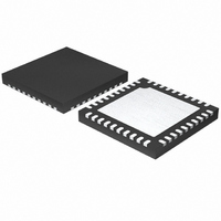
ISL6334ACRZ Intersil, ISL6334ACRZ Datasheet - Page 27

ISL6334ACRZ
Manufacturer Part Number
ISL6334ACRZ
Description
IC CTRLR PWM 4PHASE BUCK 40-QFN
Manufacturer
Intersil
Datasheet
1.ISL6334ACRZ.pdf
(30 pages)
Specifications of ISL6334ACRZ
Applications
Controller, Intel VR11.1
Voltage - Input
3 ~ 12 V
Number Of Outputs
1
Voltage - Output
0.5 ~ 1.6 V
Operating Temperature
0°C ~ 70°C
Mounting Type
Surface Mount
Package / Case
40-VFQFN, 40-VFQFPN
Lead Free Status / RoHS Status
Lead free / RoHS Compliant
Available stocks
Company
Part Number
Manufacturer
Quantity
Price
Company:
Part Number:
ISL6334ACRZ
Manufacturer:
INTERSIL
Quantity:
250
Part Number:
ISL6334ACRZ
Manufacturer:
INTERSIL
Quantity:
20 000
Part Number:
ISL6334ACRZ-T
Manufacturer:
INTERSIL
Quantity:
20 000
The feedback resistor, R
outlined in “Load-Line Regulation Resistor” on page 26.
Select a target bandwidth for the compensated system, f
The target bandwidth must be large enough to assure
adequate transient performance, but smaller than 1/3 of the
per-channel switching frequency. The values of the
compensation components depend on the relationships of f
to the L-C pole frequency and the ESR zero frequency. For
each of the three cases which follow, there is a separate set
of equations for the compensation components.
In Equation 35, L is the per-channel filter inductance divided
by the number of active channels; C is the sum total of all
output capacitors; ESR is the equivalent-series resistance of
the bulk output-filter capacitance; and V
amplitude described in the “Electrical Specifications” table
beginning on page 8.
Case 1:
Case 2:
Case 3:
FIGURE 17. COMPENSATION CONFIGURATION FOR
R
FB
LOAD-LINE REGULATED ISL6334, ISL6334A
CIRCUIT
-------------------
2π LC
R
C
f
R
C
0
C
C
-------------------
2π LC
R
C
C
C
V
>
1
+
-
C
C
DROOP
=
=
R
----------------------------- -
2πC ESR
=
=
1
C
=
=
R
--------------------------------------------------------------
(
R
0.75V
------------------------------------------------ -
2π
2πV
≤
FB
C
R
-------------------------------------
2πV
FB
FB
(
2
f
1
>
FB
)
0
C
V
--------------------------------------------- -
2
(OPTIONAL)
0.75V
f
, has already been chosen as
<
----------------------------------------- -
0.75 V
P-P
C
0
P-P
P-P
f
2πf
------------------------------------- -
IN
0
27
----------------------------- -
2πC ESR
0.75V
2
2π f
)
0.75 V
(
R
V
0.75V
(
R
ESR
0
2π
FB
P-P
IN
V
FB
0
IN
(
1
V
P-P
COMP
VDIFF
)
f
IN
2
f
R
P-P
0
(
) C
0
IN
ESR
IN
f
FB
FB
0
L
2
L
LC
)
LC
PP
LC
)
is the sawtooth
(EQ. 35)
ISL6334, ISL6334A
0
.
0
The optional capacitor C
noise away from the PWM comparator. Keep a position
available for C
capacitor of between 10pF and 100pF in case any
leading-edge jitter problem is noted.
Once selected, the compensation values in Equation 35
assure a stable converter with reasonable transient
performance. In most cases, transient performance can be
improved by making adjustments to R
value of R
oscilloscope until no further improvement is noted. Normally,
C
Equation 35 unless some performance issue is noted.
Output Filter Design
The output inductors and the output capacitor bank together
to form a low-pass filter responsible for smoothing the
pulsating voltage at the phase nodes. The output filter also
must provide the transient energy until the regulator can
respond. Because it has a low bandwidth compared to the
switching frequency, the output filter necessarily limits the
system transient response. The output capacitor must
supply or sink load current while the current in the output
inductors increases or decreases to meet the demand.
In high-speed converters, the output capacitor bank is usually
the most costly (and often the largest) part of the circuit.
Output filter design begins with minimizing the cost of this part
of the circuit. The critical load parameters in choosing the
output capacitors are the maximum size of the load step, ΔI;
the load-current slew rate, di/dt; and the maximum allowable
output-voltage deviation under transient loading, ΔV
Capacitors are characterized according to their capacitance,
ESR, and ESL (equivalent series inductance).
At the beginning of the load transient, the output capacitors
supply all of the transient current. The output voltage will initially
deviate by an amount approximated by the voltage drop across
the ESL. As the load current increases, the voltage drop across
the ESR increases linearly until the load current reaches its final
value. The capacitors selected must have sufficiently low ESL
and ESR so that the total output-voltage deviation is less than
the allowable maximum. Neglecting the contribution of inductor
current and regulator response, the output voltage initially
deviates by an amount, as shown in Equation 36:
The filter capacitor must have sufficiently low ESL and ESR
so that ΔV < ΔV
Most capacitor solutions rely on a mixture of high-frequency
capacitors with relatively low capacitance in combination
with bulk capacitors having high capacitance but limited
high-frequency performance. Minimizing the ESL of the
high-frequency capacitors allows them to support the output
voltage as the current increases. Minimizing the ESR of the
ΔV
C
will not need adjustment. Keep the value of C
≈
(
ESL
C
)
di
---- -
dt
while observing the transient performance on an
+
2
, and be prepared to install a high-frequency
(
MAX
ESR
.
) ΔI
2
, is sometimes needed to bypass
C
. Slowly increase the
C
MAX
May 28, 2009
from
(EQ. 36)
FN6482.1
.


