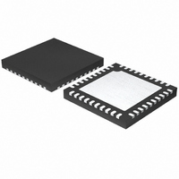
ISL6334ACRZ Intersil, ISL6334ACRZ Datasheet - Page 29

ISL6334ACRZ
Manufacturer Part Number
ISL6334ACRZ
Description
IC CTRLR PWM 4PHASE BUCK 40-QFN
Manufacturer
Intersil
Datasheet
1.ISL6334ACRZ.pdf
(30 pages)
Specifications of ISL6334ACRZ
Applications
Controller, Intel VR11.1
Voltage - Input
3 ~ 12 V
Number Of Outputs
1
Voltage - Output
0.5 ~ 1.6 V
Operating Temperature
0°C ~ 70°C
Mounting Type
Surface Mount
Package / Case
40-VFQFN, 40-VFQFPN
Lead Free Status / RoHS Status
Lead free / RoHS Compliant
Available stocks
Company
Part Number
Manufacturer
Quantity
Price
Company:
Part Number:
ISL6334ACRZ
Manufacturer:
INTERSIL
Quantity:
250
Part Number:
ISL6334ACRZ
Manufacturer:
INTERSIL
Quantity:
20 000
Part Number:
ISL6334ACRZ-T
Manufacturer:
INTERSIL
Quantity:
20 000
MULTIPHASE RMS IMPROVEMENT
Figure 21 is provided as a reference to demonstrate the
dramatic reductions in input-capacitor RMS current upon the
implementation of the multiphase topology. For example,
compare the input RMS current requirements of a 2-phase
converter versus that of a single phase. Assume both
converters have a duty cycle of 0.25, maximum sustained
output current of 40A, and a ratio of I
single phase converter would require 17.3A
capacity while the 2-phase converter would only require
10.9A
when output current is increased and additional phases are
added to keep the component cost down relative to the
single phase approach.
Intersil products are sold by description only. Intersil Corporation reserves the right to make changes in circuit design, software and/or specifications at any time without
notice. Accordingly, the reader is cautioned to verify that data sheets are current before placing orders. Information furnished by Intersil is believed to be accurate and
reliable. However, no responsibility is assumed by Intersil or its subsidiaries for its use; nor for any infringements of patents or other rights of third parties which may result
from its use. No license is granted by implication or otherwise under any patent or patent rights of Intersil or its subsidiaries.
FIGURE 21. NORMALIZED INPUT-CAPACITOR RMS
FIGURE 20. NORMALIZED INPUT-CAPACITOR RMS CURRENT
0.6
0.4
0.2
RMS
0.3
0.2
0.1
0
0
0
0
I
I
L(P-P)
L(P-P)
. The advantages become even more pronounced
vs DUTY CYCLE FOR 4-PHASE CONVERTER
CURRENT vs DUTY CYCLE FOR SINGLE-PHASE
CONVERTER
All Intersil U.S. products are manufactured, assembled and tested utilizing ISO9000 quality systems.
= 0
= 0.25 I
I
I
I
L(P-P)
L(P-P)
L(P-P)
0.2
0.2
Intersil Corporation’s quality certifications can be viewed at www.intersil.com/design/quality
= 0
= 0.5 I
= 0.75 I
O
DUTY CYCLE (V
DUTY CYCLE (V
For information regarding Intersil Corporation and its products, see www.intersil.com
O
0.4
0.4
O
29
I
I
L(P-P)
L(P-P)
0.6
= 0.5 I
= 0.75 I
0.6
O/
O/
L(P-P)
V
V
IN
IN
O
)
)
O
to I
RMS
0.8
0.8
O
of 0.5. The
current
ISL6334, ISL6334A
1.0
1.0
Layout Considerations
The following layout strategies are intended to minimize the
impact of board parasitic impedances on converter
performance and to optimize the heat-dissipating capabilities
of the printed-circuit board. These sections highlight some
important practices which should not be overlooked during the
layout process.
Component Placement
Within the allotted implementation area, orient the switching
components first. The switching components are the most
critical because they carry large amounts of energy and tend
to generate high levels of noise. Switching component
placement should take into account power dissipation. Align
the output inductors and MOSFETs such that space between
the components is minimized while creating the PHASE
plane. Place the Intersil MOSFET driver IC as close as
possible to the MOSFETs they control to reduce the parasitic
impedances due to trace length between critical driver input
and output signals. If possible, duplicate the same placement
of these components for each phase.
Next, place the input and output capacitors. Position one
high-frequency ceramic input capacitor next to each upper
MOSFET drain. Place the bulk input capacitors as close to the
upper MOSFET drains as dictated by the component size and
dimensions. Long distances between input capacitors and
MOSFET drains result in too much trace inductance and a
reduction in capacitor performance. Locate the output
capacitors between the inductors and the load, while keeping
them in close proximity to the microprocessor socket.
Voltage-Regulator (VR) Design Materials
The tolerance band calculation (TOB) worksheets for VR
output regulation and IMON have been developed using the
Root-Sum-Squared (RSS) method with 3 sigma distribution
point of the related components and parameters. Note that
the “Electrical Specifications” table beginning on page 8
specifies no less than 6 sigma distribution point, not suitable
for RSS TOB calculation. Intersil also developed a set of
worksheets to support VR design and layout. Contact
Intersil’s local office or field support for the latest available
information.
May 28, 2009
FN6482.1


