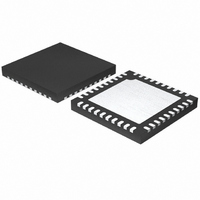
ISL6334ACRZ Intersil, ISL6334ACRZ Datasheet - Page 13

ISL6334ACRZ
Manufacturer Part Number
ISL6334ACRZ
Description
IC CTRLR PWM 4PHASE BUCK 40-QFN
Manufacturer
Intersil
Datasheet
1.ISL6334ACRZ.pdf
(30 pages)
Specifications of ISL6334ACRZ
Applications
Controller, Intel VR11.1
Voltage - Input
3 ~ 12 V
Number Of Outputs
1
Voltage - Output
0.5 ~ 1.6 V
Operating Temperature
0°C ~ 70°C
Mounting Type
Surface Mount
Package / Case
40-VFQFN, 40-VFQFPN
Lead Free Status / RoHS Status
Lead free / RoHS Compliant
Available stocks
Company
Part Number
Manufacturer
Quantity
Price
Company:
Part Number:
ISL6334ACRZ
Manufacturer:
INTERSIL
Quantity:
250
Part Number:
ISL6334ACRZ
Manufacturer:
INTERSIL
Quantity:
20 000
Part Number:
ISL6334ACRZ-T
Manufacturer:
INTERSIL
Quantity:
20 000
To understand the reduction of ripple current amplitude in the
multiphase circuit, examine Equation 1, which represents an
individual channel’s peak-to-peak inductor current.
In Equation 1, V
voltages respectively, L is the single-channel inductor value,
and F
The output capacitors conduct the ripple component of the
inductor current. In the case of multiphase converters, the
capacitor current is the sum of the ripple currents from each
of the individual channels. Compare Equation 1 to the
expression for the peak-to-peak current after the summation
of N symmetrically phase-shifted inductor currents in
Equation 2. Peak-to-peak ripple current decreases by an
amount proportional to the number of channels. Output
voltage ripple is a function of capacitance, capacitor
equivalent series resistance (ESR), and inductor ripple
current. Reducing the inductor ripple current allows the
designer to use fewer or less costly output capacitors.
Another benefit of interleaving is to reduce input ripple
current. Input capacitance is determined in part by the
maximum input ripple current. Multiphase topologies can
improve overall system cost and size by lowering input ripple
current and allowing the designer to reduce the cost of input
capacitance. The example in Figure 2 illustrates input
currents from a three-phase converter combining to reduce
the total input ripple current.
The converter depicted in Figure 2 delivers 36A to a 1.5V load
from a 12V input. The RMS input capacitor current is 5.9A.
Compare this to a single-phase converter also stepping down
12V to 1.5V at 36A. The single-phase converter has 11.9A
input capacitor current. The single-phase converter must use
I
I
PP
C PP
,
FIGURE 2. CHANNEL INPUT CURRENTS AND INPUT-
=
SW
=
(
----------------------------------------------------- -
V
(
----------------------------------------------------------- -
IN
V
INPUT-CAPACITOR CURRENT, 10A/DIV
is the switching frequency.
IN
L F
–
V
–
SW
CAPACITOR RMS CURRENT FOR 3-PHASE
CONVERTER
OUT
N V
L f
CHANNEL 3
INPUT CURRENT
10A/DIV
IN
V
S
OUT
) V
IN
V
and V
IN
OUT
CHANNEL 2
INPUT CURRENT
10A/DIV
) V
OUT
OUT
CHANNEL 1
INPUT CURRENT
10A/DIV
13
1µs/DIV
are the input and output
ISL6334, ISL6334A
(EQ. 2)
(EQ. 1)
RMS
an input capacitor bank with twice the RMS current capacity as
the equivalent three-phase converter.
Figures 18, 19 and 20 in the section entitled “” on page 28
can be used to determine the input capacitor RMS current
based on load current, duty cycle, and the number of
channels. They are provided as aids in determining the
optimal input capacitor solution. Figure 21 shows the single
phase input-capacitor RMS current for comparison.
PWM Modulation Scheme
The ISL6334, ISL6334A adopts Intersil's proprietary Active
Pulse Positioning (APP) modulation scheme to improve
transient performance. APP control is a unique dual-edge
PWM modulation scheme with both PWM leading and
trailing edges being independently moved to give the best
response to transient loads. The PWM frequency, however,
is constant and set by the external resistor between the FS
pin and GND. To further improve the transient response, the
ISL6334, ISL6334A also implements Intersil's proprietary
Adaptive Phase Alignment (APA) technique. APA, with
sufficiently large load step currents, can turn on all phases
together. With both APP and APA control, ISL6334,
ISL6334A can achieve excellent transient performance and
reduce demand on the output capacitors.
Under steady state conditions, the operation of the ISL6334,
ISL6334A PWM modulators appear to be that of a
conventional trailing edge modulator. Conventional analysis
and design methods can therefore be used for steady state
and small signal operation.
PWM and PSI# Operation
The timing of each channel is set by the number of active
channels. The default channel setting for the ISL6334,
ISL6334A is four. The switching cycle is defined as the time
between PWM pulse termination signals of each channel.
The cycle time of the pulse signal is the inverse of the
switching frequency set by the resistor between the FS pin
and ground. The PWM signals command the MOSFET
driver to turn on/off the channel MOSFETs.
For 4-channel operation, the channel firing order is 1-2-3-4:
PWM3 pulse happens 1/4 of a cycle after PWM4, PWM2
output follows another 1/4 of a cycle after PWM3, and
PWM1 delays another 1/4 of a cycle after PWM2. For
3-channel operation, the channel firing order is 1-2-3.
Connecting PWM4 to VCC selects three channel operation
and the pulse times are spaced in 1/3 cycle increments. If
PWM3 is connected to VCC, two channel operation is
selected and the PWM2 pulse happens 1/2 of a cycle after
PWM1 pulse. If PWM2 is connected to VCC, only Channel 1
operation is selected. In addition, tie PSI# to GND to
configure for single or 2-phase operation with diode
emulation on remaining channel(s), Channel 1 or Channels
1 and 3.
May 28, 2009
FN6482.1


