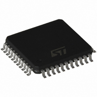
ST72F324BJ6T6 STMicroelectronics, ST72F324BJ6T6 Datasheet - Page 87

ST72F324BJ6T6
Manufacturer Part Number
ST72F324BJ6T6
Description
IC MCU 8BIT 32K FLASH 44-LQFP
Manufacturer
STMicroelectronics
Series
ST7r
Datasheet
1.ST72F324BJ2T6.pdf
(198 pages)
Specifications of ST72F324BJ6T6
Core Processor
ST7
Core Size
8-Bit
Speed
8MHz
Connectivity
SCI, SPI
Peripherals
LVD, POR, PWM, WDT
Number Of I /o
32
Program Memory Size
32KB (32K x 8)
Program Memory Type
FLASH
Ram Size
1K x 8
Voltage - Supply (vcc/vdd)
3.8 V ~ 5.5 V
Data Converters
A/D 12x10b
Oscillator Type
Internal
Operating Temperature
-40°C ~ 85°C
Package / Case
44-TQFP, 44-VQFP
Processor Series
ST72F3x
Core
ST7
Data Bus Width
8 bit
Data Ram Size
1 KB
Interface Type
SCI, SPI
Maximum Clock Frequency
8 MHz
Number Of Programmable I/os
32
Number Of Timers
3
Maximum Operating Temperature
+ 85 C
Mounting Style
SMD/SMT
Development Tools By Supplier
ST7232X-EVAL, ST7MDT20-DVP3, ST7MDT20J-EMU3, STX-RLINK
Minimum Operating Temperature
- 40 C
On-chip Adc
10 bit, 12 Channel
For Use With
497-6421 - BOARD EVAL DGTL BATT CHGR DESIGN497-5046 - KIT TOOL FOR ST7/UPSD/STR7 MCU
Lead Free Status / RoHS Status
Lead free / RoHS Compliant
Eeprom Size
-
Lead Free Status / Rohs Status
Details
Other names
497-5590
Available stocks
Company
Part Number
Manufacturer
Quantity
Price
Company:
Part Number:
ST72F324BJ6T6
Manufacturer:
ON
Quantity:
301
Company:
Part Number:
ST72F324BJ6T6
Manufacturer:
STMicroelectronics
Quantity:
10 000
Company:
Part Number:
ST72F324BJ6T6TR
Manufacturer:
STMicroelectronics
Quantity:
10 000
ST72324B-Auto
Note:
1
2
3
4
5
Figure 47. Pulse width modulation cycle
If OLVL1 = 1 and OLVL2 = 0, the length of the positive pulse is the difference between the
OC2R and OC1R registers.
If OLVL1 = OLVL2, a continuous signal will be seen on the OCMP1 pin.
The OC1R register value required for a specific timing application can be calculated using
the following formula:
Where:
t
f
PRESC = Timer prescaler factor (2, 4 or 8 depending on the CC[1:0] bits; see
If the timer clock is an external clock the formula is:
Where:
t
f
The Output Compare 2 event causes the counter to be initialized to FFFCh (see
After a write instruction to the OCiHR register, the output compare function is inhibited until
the OCiLR register is also written.
The OCF1 and OCF2 bits cannot be set by hardware in PWM mode therefore the Output
Compare interrupt is inhibited.
The ICF1 bit is set by hardware when the counter reaches the OC2R value and can produce
a timer interrupt if the ICIE bit is set and the I bit is cleared.
In PWM mode the ICAP1 pin can not be used to perform input capture because it is
disconnected to the timer. The ICAP2 pin can be used to perform input capture (ICF2 can be
set and IC2R can be loaded) but the user must take care that the counter is reset each
period and ICF1 can also generates interrupt if ICIE is set.
When the Pulse Width Modulation (PWM) and One Pulse Mode (OPM) bits are both set, the
PWM mode is the only active one.
CPU
EXT
= Signal or pulse period (in seconds)
= CPU clock frequnency (in hertz)
= Signal or pulse period (in seconds)
= External timer clock frequency (in hertz)
OCiR = t
OCiR value =
Doc ID13466 Rev 4
= OC1R
counter
= OC2R
counter
When
When
*
f
EXT
- 5
t
PRESC
*
f
OCMP1 = OLVL1
OCMP1 = OLVL2
CPU
counter is reset
ICF1 bit is set
to FFFCh
- 5
On-chip peripherals
Table
Table
50)
87/198
46).


