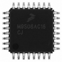
MC9S08AC16CFJE Freescale Semiconductor, MC9S08AC16CFJE Datasheet - Page 177

MC9S08AC16CFJE
Manufacturer Part Number
MC9S08AC16CFJE
Description
IC MCU 8BIT 16K FLASH 32-LQFP
Manufacturer
Freescale Semiconductor
Series
HCS08r
Specifications of MC9S08AC16CFJE
Core Processor
HCS08
Core Size
8-Bit
Speed
40MHz
Connectivity
I²C, SCI, SPI
Peripherals
LVD, POR, PWM, WDT
Number Of I /o
22
Program Memory Size
16KB (16K x 8)
Program Memory Type
FLASH
Ram Size
1K x 8
Voltage - Supply (vcc/vdd)
2.7 V ~ 5.5 V
Data Converters
A/D 6x10b
Oscillator Type
Internal
Operating Temperature
-40°C ~ 85°C
Package / Case
32-LQFP
Processor Series
S08AC
Core
HCS08
Data Bus Width
8 bit
Data Ram Size
1 KB
Interface Type
SCI/SPI
Maximum Clock Frequency
40 MHz
Number Of Programmable I/os
22
Number Of Timers
8
Maximum Operating Temperature
+ 85 C
Mounting Style
SMD/SMT
3rd Party Development Tools
EWS08
Development Tools By Supplier
DEMO9S08AC60E, DEMOACEX, DEMOACKIT, DCF51AC256, DC9S08AC128, DC9S08AC16, DC9S08AC60, DEMO51AC256KIT
Minimum Operating Temperature
- 40 C
On-chip Adc
6-ch x 10-bit
Lead Free Status / RoHS Status
Lead free / RoHS Compliant
Eeprom Size
-
Lead Free Status / Rohs Status
Lead free / RoHS Compliant
Available stocks
Company
Part Number
Manufacturer
Quantity
Price
Company:
Part Number:
MC9S08AC16CFJE
Manufacturer:
Freescale Semiconductor
Quantity:
10 000
Company:
Part Number:
MC9S08AC16CFJER
Manufacturer:
Freescale Semiconductor
Quantity:
10 000
- Current page: 177 of 336
- Download datasheet (7Mb)
(becomes unlatched) when the TPMxCnSC register is written (whether BDM mode is active or not). Any
write to the channel registers will be ignored during the input capture mode.
When BDM is active, the coherency mechanism is frozen (unless reset by writing to TPMxCnSC register)
such that the buffer latches remain in the state they were in when the BDM became active, even if one or
both halves of the channel register are read while BDM is active. This assures that if the user was in the
middle of reading a 16-bit register when BDM became active, it will read the appropriate value from the
other half of the 16-bit value after returning to normal execution. The value read from the TPMxCnVH
and TPMxCnVL registers in BDM mode is the value of these registers and not the value of their read
buffer.
In output compare or PWM modes, writing to either byte (TPMxCnVH or TPMxCnVL) latches the value
into a buffer. After both bytes are written, they are transferred as a coherent 16-bit value into the
timer-channel registers according to the value of CLKSB:CLKSA bits and the selected mode, so:
The latching mechanism may be manually reset by writing to the TPMxCnSC register (whether BDM
mode is active or not). This latching mechanism allows coherent 16-bit writes in either big-endian or
little-endian order which is friendly to various compiler implementations.
When BDM is active, the coherency mechanism is frozen such that the buffer latches remain in the state
they were in when the BDM became active even if one or both halves of the channel register are written
while BDM is active. Any write to the channel registers bypasses the buffer latches and directly write to
the channel register while BDM is active. The values written to the channel register while BDM is active
are used for PWM & output compare operation once normal execution resumes. Writes to the channel
registers while BDM is active do not interfere with partial completion of a coherency sequence. After the
coherency mechanism has been fully exercised, the channel registers are updated using the buffered values
written (while BDM was not active) by the user.
10.6
All TPM functions are associated with a central 16-bit counter which allows flexible selection of the clock
source and prescale factor. There is also a 16-bit modulo register associated with the main counter.
The CPWMS control bit chooses between center-aligned PWM operation for all channels in the TPM
(CPWMS=1) or general purpose timing functions (CPWMS=0) where each channel can independently be
configured to operate in input capture, output compare, or edge-aligned PWM mode. The CPWMS control
bit is located in the main TPM status and control register because it affects all channels within the TPM
and influences the way the main counter operates. (In CPWM mode, the counter changes to an up/down
mode rather than the up-counting mode used for general purpose timer functions.)
Freescale Semiconductor
•
•
•
If (CLKSB:CLKSA = 0:0), then the registers are updated when the second byte is written.
If (CLKSB:CLKSA not = 0:0 and in output compare mode) then the registers are updated after the
second byte is written and on the next change of the TPM counter (end of the prescaler counting).
If (CLKSB:CLKSA not = 0:0 and in EPWM or CPWM modes), then the registers are updated after
the both bytes were written, and the TPM counter changes from (TPMxMODH:TPMxMODL - 1)
to (TPMxMODH:TPMxMODL). If the TPM counter is a free-running counter then the update is
made when the TPM counter changes from 0xFFFE to 0xFFFF.
Functional Description
MC9S08AC16 Series Data Sheet, Rev. 8
Timer/PWM Module (S08TPMV3)
177
Related parts for MC9S08AC16CFJE
Image
Part Number
Description
Manufacturer
Datasheet
Request
R
Part Number:
Description:
Manufacturer:
Freescale Semiconductor, Inc
Datasheet:
Part Number:
Description:
Manufacturer:
Freescale Semiconductor, Inc
Datasheet:
Part Number:
Description:
Manufacturer:
Freescale Semiconductor, Inc
Datasheet:
Part Number:
Description:
Manufacturer:
Freescale Semiconductor, Inc
Datasheet:
Part Number:
Description:
Manufacturer:
Freescale Semiconductor, Inc
Datasheet:
Part Number:
Description:
Manufacturer:
Freescale Semiconductor, Inc
Datasheet:
Part Number:
Description:
Manufacturer:
Freescale Semiconductor, Inc
Datasheet:
Part Number:
Description:
Manufacturer:
Freescale Semiconductor, Inc
Datasheet:
Part Number:
Description:
Manufacturer:
Freescale Semiconductor, Inc
Datasheet:
Part Number:
Description:
Manufacturer:
Freescale Semiconductor, Inc
Datasheet:
Part Number:
Description:
Manufacturer:
Freescale Semiconductor, Inc
Datasheet:
Part Number:
Description:
Manufacturer:
Freescale Semiconductor, Inc
Datasheet:
Part Number:
Description:
Manufacturer:
Freescale Semiconductor, Inc
Datasheet:
Part Number:
Description:
Manufacturer:
Freescale Semiconductor, Inc
Datasheet:
Part Number:
Description:
Manufacturer:
Freescale Semiconductor, Inc
Datasheet:


