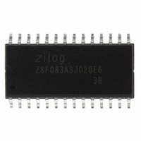
Z8F083ASJ020EG Zilog, Z8F083ASJ020EG Datasheet - Page 27

Z8F083ASJ020EG
Manufacturer Part Number
Z8F083ASJ020EG
Description
IC ENCORE XP MCU FLASH 8K 28SOIC
Manufacturer
Zilog
Series
Encore!®r
Datasheet
1.Z8F083ASJ020EG.pdf
(256 pages)
Specifications of Z8F083ASJ020EG
Core Processor
Z8
Core Size
8-Bit
Speed
20MHz
Peripherals
Brown-out Detect/Reset, LED, POR, PWM, WDT
Number Of I /o
23
Program Memory Size
8KB (8K x 8)
Program Memory Type
FLASH
Ram Size
256 x 8
Voltage - Supply (vcc/vdd)
2.7 V ~ 3.6 V
Data Converters
A/D 8x10b
Oscillator Type
Internal
Operating Temperature
-40°C ~ 105°C
Package / Case
28-SOIC (7.5mm Width)
Data Bus Width
8 bit
Data Ram Size
256 B
Maximum Clock Frequency
20 MHz
Number Of Programmable I/os
23
Number Of Timers
2
Maximum Operating Temperature
+ 105 C
Mounting Style
SMD/SMT
Minimum Operating Temperature
- 40 C
On-chip Adc
10 bit, 8 Channel
For Use With
770-1002 - ISP 4PORT ZILOG Z8 ENCORE! MCU269-4672 - KIT DEVELOPMENT F083A
Lead Free Status / RoHS Status
Lead free / RoHS Compliant
Eeprom Size
-
Connectivity
-
Lead Free Status / Rohs Status
Details
Other names
269-4558-5
Available stocks
Company
Part Number
Manufacturer
Quantity
Price
Company:
Part Number:
Z8F083ASJ020EG
Manufacturer:
Zilog
Quantity:
363
- Current page: 27 of 256
- Download datasheet (2Mb)
Address Space
Register File
Program Memory
PS026308-1207
The eZ8 CPU accesses three distinct address spaces as follows:
•
•
•
The following sections describe about these three address spaces. For more detailed
information on the eZ8 CPU and its address space, refer to eZ8 CPU User Manual
available for download at www.zilog.com.
The Register File address space in the Z8 Encore! MCU is 4 KB (4096 bytes). The
Register File consists of two sections: control registers and general purpose registers.
When instructions are executed, registers defined as source are read and registers defined
as destinations are written. The architecture of the eZ8 CPU allows all general purpose
registers to function as accumulators, address pointers, index registers, stack areas, or
scratch pad memory.
The upper 256 bytes of the 4 KB Register File address space are reserved for control of the
eZ8 CPU, on-chip peripherals, and the I/O ports. These registers are located at addresses
from
reserved (unavailable). Reading from a reserved Register File address returns an
undefined value. Writing to reserved Register File addresses is not recommended and
produces unpredictable results.
The on-chip RAM always begins at address
Z8 Encore! F083A Series devices contain up to 256 B of on-chip RAM. Reading from
Register File addresses outside the available RAM addresses (and not within the control
register address space), returns an undefined value. Writing to these Register File
addresses has no effect.
The eZ8 CPU supports 64 KB of program memory address space. The Z8 Encore! F083A
Series devices contain 1 KB to 12 KB of on-chip Flash memory in the program memory
address space, depending on the device. Reading from program memory addresses outside
The Register File addresses access for the general purpose registers and the eZ8 CPU,
peripheral, and GPIO port control registers.
The Program Memory addresses access for all the memory locations having executable
code and/or data.
The Data Memory addresses access for all the memory locations containing only the data.
F00H
to
FFFH
. Some of the addresses within the 256 B control register section are
000H
in the Register File address space. The
Z8 Encore!
Product Specification
®
F083A Series
Address Space
15
Related parts for Z8F083ASJ020EG
Image
Part Number
Description
Manufacturer
Datasheet
Request
R

Part Number:
Description:
Communication Controllers, ZILOG INTELLIGENT PERIPHERAL CONTROLLER (ZIP)
Manufacturer:
Zilog, Inc.
Datasheet:

Part Number:
Description:
KIT DEV FOR Z8 ENCORE 16K TO 64K
Manufacturer:
Zilog
Datasheet:

Part Number:
Description:
KIT DEV Z8 ENCORE XP 28-PIN
Manufacturer:
Zilog
Datasheet:

Part Number:
Description:
DEV KIT FOR Z8 ENCORE 8K/4K
Manufacturer:
Zilog
Datasheet:

Part Number:
Description:
KIT DEV Z8 ENCORE XP 28-PIN
Manufacturer:
Zilog
Datasheet:

Part Number:
Description:
DEV KIT FOR Z8 ENCORE 4K TO 8K
Manufacturer:
Zilog
Datasheet:

Part Number:
Description:
CMOS Z8 microcontroller. ROM 16 Kbytes, RAM 256 bytes, speed 16 MHz, 32 lines I/O, 3.0V to 5.5V
Manufacturer:
Zilog, Inc.
Datasheet:

Part Number:
Description:
Low-cost microcontroller. 512 bytes ROM, 61 bytes RAM, 8 MHz
Manufacturer:
Zilog, Inc.
Datasheet:

Part Number:
Description:
Z8 4K OTP Microcontroller
Manufacturer:
Zilog, Inc.
Datasheet:

Part Number:
Description:
CMOS SUPER8 ROMLESS MCU
Manufacturer:
Zilog, Inc.
Datasheet:

Part Number:
Description:
SL1866 CMOSZ8 OTP Microcontroller
Manufacturer:
Zilog, Inc.
Datasheet:

Part Number:
Description:
SL1866 CMOSZ8 OTP Microcontroller
Manufacturer:
Zilog, Inc.
Datasheet:

Part Number:
Description:
OTP (KB) = 1, RAM = 125, Speed = 12, I/O = 14, 8-bit Timers = 2, Comm Interfaces Other Features = Por, LV Protect, Voltage = 4.5-5.5V
Manufacturer:
Zilog, Inc.
Datasheet:

Part Number:
Description:
Manufacturer:
Zilog, Inc.
Datasheet:


