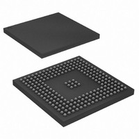
AT91SAM9260B-CU-999 Atmel, AT91SAM9260B-CU-999 Datasheet - Page 144

AT91SAM9260B-CU-999
Manufacturer Part Number
AT91SAM9260B-CU-999
Description
IC MCU ARM9 217LFBGA
Manufacturer
Atmel
Series
AT91SAMr
Datasheet
1.AT91SAM9260B-CU-999.pdf
(798 pages)
Specifications of AT91SAM9260B-CU-999
Core Processor
ARM9
Core Size
16/32-Bit
Speed
180MHz
Connectivity
EBI/EMI, Ethernet, I²C, MMC, SPI, SSC, UART/USART, USB
Peripherals
POR, WDT
Number Of I /o
96
Program Memory Size
32KB (32K x 8)
Program Memory Type
ROM
Ram Size
24K x 8
Voltage - Supply (vcc/vdd)
1.65 V ~ 1.95 V
Data Converters
A/D 4x10b
Oscillator Type
Internal
Operating Temperature
-40°C ~ 85°C
Package / Case
217-LFBGA
Processor Series
AT91SAMx
Core
ARM926EJ-S
Data Bus Width
32 bit
Data Ram Size
8 KB
Interface Type
2-Wire, EBI, I2S, SPI, USART
Maximum Clock Frequency
180 MHz
Number Of Programmable I/os
96
Number Of Timers
6
Maximum Operating Temperature
+ 85 C
Mounting Style
SMD/SMT
3rd Party Development Tools
JTRACE-ARM-2M, MDK-ARM, RL-ARM, ULINK2
Development Tools By Supplier
AT91SAM-ICE, AT91-ISP, AT91SAM9260-EK
Minimum Operating Temperature
- 40 C
On-chip Adc
10 bit, 4 Channel
For Use With
AT91SAM9260-EK - KIT EVAL FOR AT91SAM9260AT91SAM-ICE - EMULATOR FOR AT91 ARM7/ARM9
Lead Free Status / RoHS Status
Lead free / RoHS Compliant
Eeprom Size
-
Lead Free Status / Rohs Status
Details
Available stocks
Company
Part Number
Manufacturer
Quantity
Price
- Current page: 144 of 798
- Download datasheet (12Mb)
19.6.6.1
Figure 19-3. CompactFlash Memory Mapping
19.6.6.2
144
AT91SAM9260
I/O Mode, Common Memory Mode, Attribute Memory Mode and True IDE Mode
CFCE1 and CFCE2 Signals
CF Address Space
Within the NCS4 and/or NCS5 address space, the current transfer address is used to distinguish
I/O mode, common memory mode, attribute memory mode and True IDE mode.
The different modes are accessed through a specific memory mapping as illustrated on
19-3. A[23:21] bits of the transfer address are used to select the desired mode as described in
Table 19-5 on page
Note:
Table 19-5.
To cover all types of access, the SMC must be alternatively set to drive 8-bit data bus or 16-bit
data bus. The odd byte access on the D[7:0] bus is only possible when the SMC is configured to
drive 8-bit memory devices on the corresponding NCS pin (NCS4 or NCS5). The Chip Select
Register (DBW field in the corresponding Chip Select Register) of the NCS4 and/or NCS5
address space must be set as shown in
NBS1 and NBS0 are the byte selection signals from SMC and are available when the SMC is set
in Byte Select mode on the corresponding Chip Select.
A[23:21]
000
010
100
110
111
The A22 pin is used to drive the REG signal of the CompactFlash Device (except in True IDE
mode).
CompactFlash Mode Selection
Offset 0x00E0 0000
Offset 0x00C0 0000
Offset 0x0080 0000
Offset 0x0040 0000
Offset 0x0000 0000
144.
Table 19-6
Common Memory Mode Space
True IDE Alternate Mode Space
Attribute Memory Mode Space
True IDE Mode Space
I/O Mode Space
to enable the required access type.
Alternate True IDE Mode
Mode Base Address
Common Memory
Attribute Memory
True IDE Mode
I/O Mode
6221I–ATARM–17-Jul-09
Figure
Related parts for AT91SAM9260B-CU-999
Image
Part Number
Description
Manufacturer
Datasheet
Request
R

Part Number:
Description:
Manufacturer:
ATMEL Corporation
Datasheet:

Part Number:
Description:
KIT EVAL FOR AT91SAM9260
Manufacturer:
Atmel
Datasheet:

Part Number:
Description:
AT91 ARM Thumb Microcontrollers
Manufacturer:
ATMEL [ATMEL Corporation]
Datasheet:

Part Number:
Description:
AT91 ARM Thumb Microcontrollers
Manufacturer:
ATMEL Corporation
Datasheet:

Part Number:
Description:
At91 Arm Thumb Microcontrollers
Manufacturer:
ATMEL Corporation
Datasheet:

Part Number:
Description:
MCU, MPU & DSP Development Tools DEV BRD FOR AT91SAM9260
Manufacturer:
Olimex Ltd.
Datasheet:

Part Number:
Description:
MCU, MPU & DSP Development Tools KICKSTART KIT FOR AT91SAM9 PLUS
Manufacturer:
IAR Systems

Part Number:
Description:
DEV KIT FOR AVR/AVR32
Manufacturer:
Atmel
Datasheet:

Part Number:
Description:
INTERVAL AND WIPE/WASH WIPER CONTROL IC WITH DELAY
Manufacturer:
ATMEL Corporation
Datasheet:

Part Number:
Description:
Low-Voltage Voice-Switched IC for Hands-Free Operation
Manufacturer:
ATMEL Corporation
Datasheet:

Part Number:
Description:
MONOLITHIC INTEGRATED FEATUREPHONE CIRCUIT
Manufacturer:
ATMEL Corporation
Datasheet:

Part Number:
Description:
AM-FM Receiver IC U4255BM-M
Manufacturer:
ATMEL Corporation
Datasheet:

Part Number:
Description:
Monolithic Integrated Feature Phone Circuit
Manufacturer:
ATMEL Corporation
Datasheet:

Part Number:
Description:
Multistandard Video-IF and Quasi Parallel Sound Processing
Manufacturer:
ATMEL Corporation
Datasheet:


