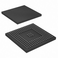
AT91SAM9260B-CU-999 Atmel, AT91SAM9260B-CU-999 Datasheet - Page 2

AT91SAM9260B-CU-999
Manufacturer Part Number
AT91SAM9260B-CU-999
Description
IC MCU ARM9 217LFBGA
Manufacturer
Atmel
Series
AT91SAMr
Datasheet
1.AT91SAM9260B-CU-999.pdf
(798 pages)
Specifications of AT91SAM9260B-CU-999
Core Processor
ARM9
Core Size
16/32-Bit
Speed
180MHz
Connectivity
EBI/EMI, Ethernet, I²C, MMC, SPI, SSC, UART/USART, USB
Peripherals
POR, WDT
Number Of I /o
96
Program Memory Size
32KB (32K x 8)
Program Memory Type
ROM
Ram Size
24K x 8
Voltage - Supply (vcc/vdd)
1.65 V ~ 1.95 V
Data Converters
A/D 4x10b
Oscillator Type
Internal
Operating Temperature
-40°C ~ 85°C
Package / Case
217-LFBGA
Processor Series
AT91SAMx
Core
ARM926EJ-S
Data Bus Width
32 bit
Data Ram Size
8 KB
Interface Type
2-Wire, EBI, I2S, SPI, USART
Maximum Clock Frequency
180 MHz
Number Of Programmable I/os
96
Number Of Timers
6
Maximum Operating Temperature
+ 85 C
Mounting Style
SMD/SMT
3rd Party Development Tools
JTRACE-ARM-2M, MDK-ARM, RL-ARM, ULINK2
Development Tools By Supplier
AT91SAM-ICE, AT91-ISP, AT91SAM9260-EK
Minimum Operating Temperature
- 40 C
On-chip Adc
10 bit, 4 Channel
For Use With
AT91SAM9260-EK - KIT EVAL FOR AT91SAM9260AT91SAM-ICE - EMULATOR FOR AT91 ARM7/ARM9
Lead Free Status / RoHS Status
Lead free / RoHS Compliant
Eeprom Size
-
Lead Free Status / Rohs Status
Details
Available stocks
Company
Part Number
Manufacturer
Quantity
Price
- Current page: 2 of 798
- Download datasheet (12Mb)
1. Description
2. AT91SAM9260 Block Diagram
2
AT91SAM9260
The AT91SAM9260 is based on the integration of an ARM926EJ-S processor with fast ROM
and RAM memories and a wide range of peripherals.
The AT91SAM9260 embeds an Ethernet MAC, one USB Device Port, and a USB Host control-
ler. It also integrates several standard peripherals, such as the USART, SPI, TWI, Timer
Counters, Synchronous Serial Controller, ADC and MultiMedia Card Interface.
The AT91SAM9260 is architectured on a 6-layer matrix, allowing a maximum internal bandwidth
of six 32-bit buses. It also features an External Bus Interface capable of interfacing with a wide
range of memory devices.
The block diagram shows all the features for the 217-LFBGA package. Some functions are not
accessible in the 208-pin PQFP package and the unavailable pins are highlighted in
ing on PIO Controller A” on page
“Multiplexing on PIO Controller C” on page
pin package.
able in the 208-PQFP package.
Table 2-1.
PC12
PB12
PB13
PA30
PA31
PC2
PC3
PIO
-
-
Table 2-1 on page 2
Unavailable Signals in 208-lead PQFP Package
defines all the multiplexed and not multiplexed pins not avail-
Peripheral A
27,
HDMB
HDPB
SCK2
SCK0
TXD5
RXD5
IRQ0
AD2
AD3
“Multiplexing on PIO Controller B” on page
29. The USB Host Port B is not available in the 208-
SPI1_NPCS3
Peripheral B
ISI_D10
ISI_D11
RXD4
PCK1
NCS7
TXD4
-
-
6221I–ATARM–17-Jul-09
“Multiplex-
28,
Related parts for AT91SAM9260B-CU-999
Image
Part Number
Description
Manufacturer
Datasheet
Request
R

Part Number:
Description:
Manufacturer:
ATMEL Corporation
Datasheet:

Part Number:
Description:
KIT EVAL FOR AT91SAM9260
Manufacturer:
Atmel
Datasheet:

Part Number:
Description:
AT91 ARM Thumb Microcontrollers
Manufacturer:
ATMEL [ATMEL Corporation]
Datasheet:

Part Number:
Description:
AT91 ARM Thumb Microcontrollers
Manufacturer:
ATMEL Corporation
Datasheet:

Part Number:
Description:
At91 Arm Thumb Microcontrollers
Manufacturer:
ATMEL Corporation
Datasheet:

Part Number:
Description:
MCU, MPU & DSP Development Tools DEV BRD FOR AT91SAM9260
Manufacturer:
Olimex Ltd.
Datasheet:

Part Number:
Description:
MCU, MPU & DSP Development Tools KICKSTART KIT FOR AT91SAM9 PLUS
Manufacturer:
IAR Systems

Part Number:
Description:
DEV KIT FOR AVR/AVR32
Manufacturer:
Atmel
Datasheet:

Part Number:
Description:
INTERVAL AND WIPE/WASH WIPER CONTROL IC WITH DELAY
Manufacturer:
ATMEL Corporation
Datasheet:

Part Number:
Description:
Low-Voltage Voice-Switched IC for Hands-Free Operation
Manufacturer:
ATMEL Corporation
Datasheet:

Part Number:
Description:
MONOLITHIC INTEGRATED FEATUREPHONE CIRCUIT
Manufacturer:
ATMEL Corporation
Datasheet:

Part Number:
Description:
AM-FM Receiver IC U4255BM-M
Manufacturer:
ATMEL Corporation
Datasheet:

Part Number:
Description:
Monolithic Integrated Feature Phone Circuit
Manufacturer:
ATMEL Corporation
Datasheet:

Part Number:
Description:
Multistandard Video-IF and Quasi Parallel Sound Processing
Manufacturer:
ATMEL Corporation
Datasheet:


