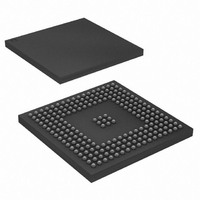
AT91SAM9260B-CU-999 Atmel, AT91SAM9260B-CU-999 Datasheet - Page 765

AT91SAM9260B-CU-999
Manufacturer Part Number
AT91SAM9260B-CU-999
Description
IC MCU ARM9 217LFBGA
Manufacturer
Atmel
Series
AT91SAMr
Datasheet
1.AT91SAM9260B-CU-999.pdf
(798 pages)
Specifications of AT91SAM9260B-CU-999
Core Processor
ARM9
Core Size
16/32-Bit
Speed
180MHz
Connectivity
EBI/EMI, Ethernet, I²C, MMC, SPI, SSC, UART/USART, USB
Peripherals
POR, WDT
Number Of I /o
96
Program Memory Size
32KB (32K x 8)
Program Memory Type
ROM
Ram Size
24K x 8
Voltage - Supply (vcc/vdd)
1.65 V ~ 1.95 V
Data Converters
A/D 4x10b
Oscillator Type
Internal
Operating Temperature
-40°C ~ 85°C
Package / Case
217-LFBGA
Processor Series
AT91SAMx
Core
ARM926EJ-S
Data Bus Width
32 bit
Data Ram Size
8 KB
Interface Type
2-Wire, EBI, I2S, SPI, USART
Maximum Clock Frequency
180 MHz
Number Of Programmable I/os
96
Number Of Timers
6
Maximum Operating Temperature
+ 85 C
Mounting Style
SMD/SMT
3rd Party Development Tools
JTRACE-ARM-2M, MDK-ARM, RL-ARM, ULINK2
Development Tools By Supplier
AT91SAM-ICE, AT91-ISP, AT91SAM9260-EK
Minimum Operating Temperature
- 40 C
On-chip Adc
10 bit, 4 Channel
For Use With
AT91SAM9260-EK - KIT EVAL FOR AT91SAM9260AT91SAM-ICE - EMULATOR FOR AT91 ARM7/ARM9
Lead Free Status / RoHS Status
Lead free / RoHS Compliant
Eeprom Size
-
Lead Free Status / Rohs Status
Details
Available stocks
Company
Part Number
Manufacturer
Quantity
Price
- Current page: 765 of 798
- Download datasheet (12Mb)
43.2.13
43.2.13.1
43.2.14
43.2.14.1
43.2.15
43.2.15.1
43.2.16
43.2.16.1
6221I–ATARM–17-Jul-09
Shutdown Controller (SHDWC)
System Controller
Two-wire Interface (TWI)
UHP
SHDWC: SHDN Signal may be Driven to Low Level Voltage During Device Power-on
Possible Event Loss when Reading RTT_SR
Switch from Slave to Master Mode
Non-ISO IN Transfers
If only VDDBU is powered during boot sequence (No VDDCORE), the SHDN signal may be
driven to low level voltage after a delay.This delay is linked to the startup time of the slow clock
selected by OSCSEL signal.
If SHDN pin is connected to the Enable pin (EN) of the VDDCORE regulator, VDDCORE estab-
lishment does not occur and the system does not start.
If an event (RTTINC or ALMS) occurs within the same slow clock cycle as when the RTT_SR is
read, the corresponding bit might be cleared. This can lead to the loss of this event.
The software must handle an RTT event as an interrupt and should not poll RTT_SR.
At the end of transfer in slave mode, the slave mode is disabled, the master mode is enabled
and thus a transfer in master mode can be performed. In the current device, the start event is
correctly generated but the SCL line is stuck at 1, so no transfer is possible.
Two workarounds are possible:
or
Conditions:
Consider the following sequence:
1. VDDCORE must be established within the delay corresponding to the startup time of
2. Add a glue logic to latch the rising edge of the SHDN signal. The reset of the latch out-
1. Perform a software reset before going to master mode (TWI must be reconfigured).
2. Perform a slave read access before switching to master mode.
1. The Host controller issues an IN token.
2. The Device provides the IN data in a short packet.
3. The Host controller writes the received data to the system memory.
4. The Host controller is now supposed to carry out two Write transactions (TD status
Problem Fix/Workaround
Problem Fix/Workaround
Problem Fix/Workaround
the slow clock selected by OSCSEL.
put (EN_REG) can be connected to a PIO and used to enter the shutdown mode.
write and TD retirement write) to the system memory in order to complete the status
update.
AT91SAM9260
765
Related parts for AT91SAM9260B-CU-999
Image
Part Number
Description
Manufacturer
Datasheet
Request
R

Part Number:
Description:
Manufacturer:
ATMEL Corporation
Datasheet:

Part Number:
Description:
KIT EVAL FOR AT91SAM9260
Manufacturer:
Atmel
Datasheet:

Part Number:
Description:
AT91 ARM Thumb Microcontrollers
Manufacturer:
ATMEL [ATMEL Corporation]
Datasheet:

Part Number:
Description:
AT91 ARM Thumb Microcontrollers
Manufacturer:
ATMEL Corporation
Datasheet:

Part Number:
Description:
At91 Arm Thumb Microcontrollers
Manufacturer:
ATMEL Corporation
Datasheet:

Part Number:
Description:
MCU, MPU & DSP Development Tools DEV BRD FOR AT91SAM9260
Manufacturer:
Olimex Ltd.
Datasheet:

Part Number:
Description:
MCU, MPU & DSP Development Tools KICKSTART KIT FOR AT91SAM9 PLUS
Manufacturer:
IAR Systems

Part Number:
Description:
DEV KIT FOR AVR/AVR32
Manufacturer:
Atmel
Datasheet:

Part Number:
Description:
INTERVAL AND WIPE/WASH WIPER CONTROL IC WITH DELAY
Manufacturer:
ATMEL Corporation
Datasheet:

Part Number:
Description:
Low-Voltage Voice-Switched IC for Hands-Free Operation
Manufacturer:
ATMEL Corporation
Datasheet:

Part Number:
Description:
MONOLITHIC INTEGRATED FEATUREPHONE CIRCUIT
Manufacturer:
ATMEL Corporation
Datasheet:

Part Number:
Description:
AM-FM Receiver IC U4255BM-M
Manufacturer:
ATMEL Corporation
Datasheet:

Part Number:
Description:
Monolithic Integrated Feature Phone Circuit
Manufacturer:
ATMEL Corporation
Datasheet:

Part Number:
Description:
Multistandard Video-IF and Quasi Parallel Sound Processing
Manufacturer:
ATMEL Corporation
Datasheet:


