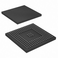
AT91SAM9260B-CU-999 Atmel, AT91SAM9260B-CU-999 Datasheet - Page 92

AT91SAM9260B-CU-999
Manufacturer Part Number
AT91SAM9260B-CU-999
Description
IC MCU ARM9 217LFBGA
Manufacturer
Atmel
Series
AT91SAMr
Datasheet
1.AT91SAM9260B-CU-999.pdf
(798 pages)
Specifications of AT91SAM9260B-CU-999
Core Processor
ARM9
Core Size
16/32-Bit
Speed
180MHz
Connectivity
EBI/EMI, Ethernet, I²C, MMC, SPI, SSC, UART/USART, USB
Peripherals
POR, WDT
Number Of I /o
96
Program Memory Size
32KB (32K x 8)
Program Memory Type
ROM
Ram Size
24K x 8
Voltage - Supply (vcc/vdd)
1.65 V ~ 1.95 V
Data Converters
A/D 4x10b
Oscillator Type
Internal
Operating Temperature
-40°C ~ 85°C
Package / Case
217-LFBGA
Processor Series
AT91SAMx
Core
ARM926EJ-S
Data Bus Width
32 bit
Data Ram Size
8 KB
Interface Type
2-Wire, EBI, I2S, SPI, USART
Maximum Clock Frequency
180 MHz
Number Of Programmable I/os
96
Number Of Timers
6
Maximum Operating Temperature
+ 85 C
Mounting Style
SMD/SMT
3rd Party Development Tools
JTRACE-ARM-2M, MDK-ARM, RL-ARM, ULINK2
Development Tools By Supplier
AT91SAM-ICE, AT91-ISP, AT91SAM9260-EK
Minimum Operating Temperature
- 40 C
On-chip Adc
10 bit, 4 Channel
For Use With
AT91SAM9260-EK - KIT EVAL FOR AT91SAM9260AT91SAM-ICE - EMULATOR FOR AT91 ARM7/ARM9
Lead Free Status / RoHS Status
Lead free / RoHS Compliant
Eeprom Size
-
Lead Free Status / Rohs Status
Details
Available stocks
Company
Part Number
Manufacturer
Quantity
Price
- Current page: 92 of 798
- Download datasheet (12Mb)
13.8
6221I–ATARM–17-Jul-09
ROM Code Change Log
The SPI and NAND Flash drivers use several PIOs in alternate functions to communicate with
devices. Care must be taken when these PIOs are used by the application. The devices con-
nected could be unintentionally driven at boot time, and electrical conflicts between SPI output
pins and the connected devices may appear.
To assure correct functionality, it is recommended to plug in critical devices to other pins.
Table 13-11
are driven during the boot sequence for a period of less than 1 second if no correct boot program
is found.
For the DataFlash driven by the SPCK signal at 1 MHz, the time to download 4096 bytes is
reduced to 200 ms.
Before performing the jump to the application in internal SRAM, all the PIOs and peripherals
used in the boot program are set to their reset state.
Table 13-11. Pins Driven during Boot Program Execution
Here are the evolutions between ROM Code V1.4 and V1.7:
Note:
Peripheral
SPI0
SPI0
SPI0
SPI0
SPI0
PIOC
DBGU
DBGU
• The DataFlash and NAND Flash downloaded code size must be inferior to 4096 bytes.
• The code is always downloaded from the device address 0x0000_0000 to the address
• The downloaded code must be position-independent or linked at address 0x0000_0000.
• The DataFlash must be connected to NPCS0 and/or NPCS1 of the SPI.
• USB requirements:
• User Reset is no longer enabled
• NAND Flash Ready/Busy pin (PIOC 13) is no longer used
• There are no more Timeouts in the NAND Flash Boot sequence
0x0000_0000 of the internal SRAM (after remap).
– Crystal or Input Frequencies supported by Software Auto-detection. See
Table 13-2
To know which ROM Code version is in the chip, use the SAM-BA Monitor command “V#” (see
Table 13-8 on page 91
contains a list of pins that are driven during the boot program execution. These pins
and
Table 13-3 on page 81
)
Pin
MOSI
MISO
SPCK
NPCS0
NPCS1
NANDCS
DRXD
DTXD
for more information.
AT91SAM9260
PIO Line
PIOC11
PIOC14
PIOB14
PIOB15
PIOA1
PIOA0
PIOA2
PIOA3
Table
13-1,
92
Related parts for AT91SAM9260B-CU-999
Image
Part Number
Description
Manufacturer
Datasheet
Request
R

Part Number:
Description:
Manufacturer:
ATMEL Corporation
Datasheet:

Part Number:
Description:
KIT EVAL FOR AT91SAM9260
Manufacturer:
Atmel
Datasheet:

Part Number:
Description:
AT91 ARM Thumb Microcontrollers
Manufacturer:
ATMEL [ATMEL Corporation]
Datasheet:

Part Number:
Description:
AT91 ARM Thumb Microcontrollers
Manufacturer:
ATMEL Corporation
Datasheet:

Part Number:
Description:
At91 Arm Thumb Microcontrollers
Manufacturer:
ATMEL Corporation
Datasheet:

Part Number:
Description:
MCU, MPU & DSP Development Tools DEV BRD FOR AT91SAM9260
Manufacturer:
Olimex Ltd.
Datasheet:

Part Number:
Description:
MCU, MPU & DSP Development Tools KICKSTART KIT FOR AT91SAM9 PLUS
Manufacturer:
IAR Systems

Part Number:
Description:
DEV KIT FOR AVR/AVR32
Manufacturer:
Atmel
Datasheet:

Part Number:
Description:
INTERVAL AND WIPE/WASH WIPER CONTROL IC WITH DELAY
Manufacturer:
ATMEL Corporation
Datasheet:

Part Number:
Description:
Low-Voltage Voice-Switched IC for Hands-Free Operation
Manufacturer:
ATMEL Corporation
Datasheet:

Part Number:
Description:
MONOLITHIC INTEGRATED FEATUREPHONE CIRCUIT
Manufacturer:
ATMEL Corporation
Datasheet:

Part Number:
Description:
AM-FM Receiver IC U4255BM-M
Manufacturer:
ATMEL Corporation
Datasheet:

Part Number:
Description:
Monolithic Integrated Feature Phone Circuit
Manufacturer:
ATMEL Corporation
Datasheet:

Part Number:
Description:
Multistandard Video-IF and Quasi Parallel Sound Processing
Manufacturer:
ATMEL Corporation
Datasheet:


