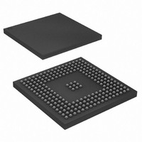
AT91SAM9260B-CU-999 Atmel, AT91SAM9260B-CU-999 Datasheet - Page 206

AT91SAM9260B-CU-999
Manufacturer Part Number
AT91SAM9260B-CU-999
Description
IC MCU ARM9 217LFBGA
Manufacturer
Atmel
Series
AT91SAMr
Datasheet
1.AT91SAM9260B-CU-999.pdf
(798 pages)
Specifications of AT91SAM9260B-CU-999
Core Processor
ARM9
Core Size
16/32-Bit
Speed
180MHz
Connectivity
EBI/EMI, Ethernet, I²C, MMC, SPI, SSC, UART/USART, USB
Peripherals
POR, WDT
Number Of I /o
96
Program Memory Size
32KB (32K x 8)
Program Memory Type
ROM
Ram Size
24K x 8
Voltage - Supply (vcc/vdd)
1.65 V ~ 1.95 V
Data Converters
A/D 4x10b
Oscillator Type
Internal
Operating Temperature
-40°C ~ 85°C
Package / Case
217-LFBGA
Processor Series
AT91SAMx
Core
ARM926EJ-S
Data Bus Width
32 bit
Data Ram Size
8 KB
Interface Type
2-Wire, EBI, I2S, SPI, USART
Maximum Clock Frequency
180 MHz
Number Of Programmable I/os
96
Number Of Timers
6
Maximum Operating Temperature
+ 85 C
Mounting Style
SMD/SMT
3rd Party Development Tools
JTRACE-ARM-2M, MDK-ARM, RL-ARM, ULINK2
Development Tools By Supplier
AT91SAM-ICE, AT91-ISP, AT91SAM9260-EK
Minimum Operating Temperature
- 40 C
On-chip Adc
10 bit, 4 Channel
For Use With
AT91SAM9260-EK - KIT EVAL FOR AT91SAM9260AT91SAM-ICE - EMULATOR FOR AT91 ARM7/ARM9
Lead Free Status / RoHS Status
Lead free / RoHS Compliant
Eeprom Size
-
Lead Free Status / Rohs Status
Details
Available stocks
Company
Part Number
Manufacturer
Quantity
Price
- Current page: 206 of 798
- Download datasheet (12Mb)
6221I–ATARM–17-Jul-09
After initialization, the SDRAM devices are fully functional.
Note:
6. An All Banks Precharge command is issued to the SDRAM devices. The application
7. Eight auto-refresh (CBR) cycles are provided. The application must set the Mode to 4 in
8. A Mode Register set (MRS) cycle is issued to program the parameters of the SDRAM
9. For mobile SDRAM initialization, an Extended Mode Register set (EMRS) cycle is
10. The application must go into Normal Mode, setting Mode to 0 in the Mode Register and
11. Write the refresh rate into the count field in the SDRAMC Refresh Timer register.
must set Mode to 2 in the Mode Register and perform a write access to any SDRAM
address.
the Mode Register and perform a write access to any SDRAM location eight times.
devices, in particular CAS latency and burst length. The application must set Mode to 3
in the Mode Register and perform a write access to the SDRAM. The write address
must be chosen so that BA[1:0] are set to 0. For example, with a 16-bit 128 MB SDRAM
(12 rows, 9 columns, 4 banks) bank address, the SDRAM write access should be done
at the address 0x20000000.
issued to program the SDRAM parameters (TCSR, PASR, DS). The application must
set Mode to 5 in the Mode Register and perform a write access to the SDRAM. The
write address must be chosen so that BA[1] or BA[0] are set to 1. For example, with a
16-bit 128 MB SDRAM, (12 rows, 9 columns, 4 banks) bank address the SDRAM write
access should be done at the address 0x20800000 or 0x20400000.
performing a write access at any location in the SDRAM.
(Refresh rate = delay between refresh cycles). The SDRAM device requires a refresh
every 15.625 µs or 7.81 µs. With a 100 MHz frequency, the Refresh Timer Counter
Register must be set with the value 1562(15.652 µs x 100 MHz) or 781(7.81 µs x 100
MHz).
1. It is strongly recommended to respect the instructions stated in
cess in order to be certain that the subsequent commands issued by the SDRAMC will be
taken into account.
AT91SAM9260
Step 5
of the initialization pro-
206
Related parts for AT91SAM9260B-CU-999
Image
Part Number
Description
Manufacturer
Datasheet
Request
R

Part Number:
Description:
Manufacturer:
ATMEL Corporation
Datasheet:

Part Number:
Description:
KIT EVAL FOR AT91SAM9260
Manufacturer:
Atmel
Datasheet:

Part Number:
Description:
AT91 ARM Thumb Microcontrollers
Manufacturer:
ATMEL [ATMEL Corporation]
Datasheet:

Part Number:
Description:
AT91 ARM Thumb Microcontrollers
Manufacturer:
ATMEL Corporation
Datasheet:

Part Number:
Description:
At91 Arm Thumb Microcontrollers
Manufacturer:
ATMEL Corporation
Datasheet:

Part Number:
Description:
MCU, MPU & DSP Development Tools DEV BRD FOR AT91SAM9260
Manufacturer:
Olimex Ltd.
Datasheet:

Part Number:
Description:
MCU, MPU & DSP Development Tools KICKSTART KIT FOR AT91SAM9 PLUS
Manufacturer:
IAR Systems

Part Number:
Description:
DEV KIT FOR AVR/AVR32
Manufacturer:
Atmel
Datasheet:

Part Number:
Description:
INTERVAL AND WIPE/WASH WIPER CONTROL IC WITH DELAY
Manufacturer:
ATMEL Corporation
Datasheet:

Part Number:
Description:
Low-Voltage Voice-Switched IC for Hands-Free Operation
Manufacturer:
ATMEL Corporation
Datasheet:

Part Number:
Description:
MONOLITHIC INTEGRATED FEATUREPHONE CIRCUIT
Manufacturer:
ATMEL Corporation
Datasheet:

Part Number:
Description:
AM-FM Receiver IC U4255BM-M
Manufacturer:
ATMEL Corporation
Datasheet:

Part Number:
Description:
Monolithic Integrated Feature Phone Circuit
Manufacturer:
ATMEL Corporation
Datasheet:

Part Number:
Description:
Multistandard Video-IF and Quasi Parallel Sound Processing
Manufacturer:
ATMEL Corporation
Datasheet:


