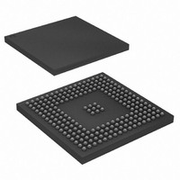
AT91SAM9260B-CU-999 Atmel, AT91SAM9260B-CU-999 Datasheet - Page 262

AT91SAM9260B-CU-999
Manufacturer Part Number
AT91SAM9260B-CU-999
Description
IC MCU ARM9 217LFBGA
Manufacturer
Atmel
Series
AT91SAMr
Datasheet
1.AT91SAM9260B-CU-999.pdf
(798 pages)
Specifications of AT91SAM9260B-CU-999
Core Processor
ARM9
Core Size
16/32-Bit
Speed
180MHz
Connectivity
EBI/EMI, Ethernet, I²C, MMC, SPI, SSC, UART/USART, USB
Peripherals
POR, WDT
Number Of I /o
96
Program Memory Size
32KB (32K x 8)
Program Memory Type
ROM
Ram Size
24K x 8
Voltage - Supply (vcc/vdd)
1.65 V ~ 1.95 V
Data Converters
A/D 4x10b
Oscillator Type
Internal
Operating Temperature
-40°C ~ 85°C
Package / Case
217-LFBGA
Processor Series
AT91SAMx
Core
ARM926EJ-S
Data Bus Width
32 bit
Data Ram Size
8 KB
Interface Type
2-Wire, EBI, I2S, SPI, USART
Maximum Clock Frequency
180 MHz
Number Of Programmable I/os
96
Number Of Timers
6
Maximum Operating Temperature
+ 85 C
Mounting Style
SMD/SMT
3rd Party Development Tools
JTRACE-ARM-2M, MDK-ARM, RL-ARM, ULINK2
Development Tools By Supplier
AT91SAM-ICE, AT91-ISP, AT91SAM9260-EK
Minimum Operating Temperature
- 40 C
On-chip Adc
10 bit, 4 Channel
For Use With
AT91SAM9260-EK - KIT EVAL FOR AT91SAM9260AT91SAM-ICE - EMULATOR FOR AT91 ARM7/ARM9
Lead Free Status / RoHS Status
Lead free / RoHS Compliant
Eeprom Size
-
Lead Free Status / Rohs Status
Details
Available stocks
Company
Part Number
Manufacturer
Quantity
Price
- Current page: 262 of 798
- Download datasheet (12Mb)
25.8
25.8.1
6221I–ATARM–17-Jul-09
Clock Switching Details
Master Clock Switching Timings
Table 25-1
from one selected clock to another one. This is in the event that the prescaler is deactivated.
When the prescaler is activated, an additional time of 64 clock cycles of the new selected clock
has to be added.
Table 25-1.
Notes:
Table 25-2.
To
Main Clock
SLCK
PLL Clock
To
PLLA Clock
PLLB Clock
1. PLL designates either the PLL A or the PLL B Clock.
2. PLLCOUNT designates either PLLACOUNT or PLLBCOUNT.
From
and
From
Clock Switching Timings (Worst Case)
Clock Switching Timings Between Two PLLs (Worst Case)
Table 25-2
PLLCOUNT x SLCK +
0.5 x Main Clock +
0.5 x Main Clock +
2.5 x PLLx Clock
Main Clock
4.5 x SLCK
4 x SLCK +
PLLACOUNT x SLCK
2.5 x PLLA Clock +
–
give the worst case timings required for the Master Clock to switch
3 x PLLB Clock +
1.5 x PLLB Clock
PLLA Clock
4 x SLCK +
4 x SLCK +
PLLCOUNT x SLCK
2.5 x PLL Clock +
2.5 x Main Clock
4 x SLCK +
5 x SLCK +
SLCK
–
PLLBCOUNT x SLCK
2.5 x PLLB Clock +
3 x PLLA Clock +
1.5 x PLLA Clock
PLLB Clock
4 x SLCK +
4 x SLCK +
PLLCOUNT x SLCK
AT91SAM9260
2.5 x PLL Clock +
3 x PLL Clock +
3 x PLL Clock +
1 x Main Clock
4 x SLCK +
4 x SLCK +
PLL Clock
5 x SLCK
262
Related parts for AT91SAM9260B-CU-999
Image
Part Number
Description
Manufacturer
Datasheet
Request
R

Part Number:
Description:
Manufacturer:
ATMEL Corporation
Datasheet:

Part Number:
Description:
KIT EVAL FOR AT91SAM9260
Manufacturer:
Atmel
Datasheet:

Part Number:
Description:
AT91 ARM Thumb Microcontrollers
Manufacturer:
ATMEL [ATMEL Corporation]
Datasheet:

Part Number:
Description:
AT91 ARM Thumb Microcontrollers
Manufacturer:
ATMEL Corporation
Datasheet:

Part Number:
Description:
At91 Arm Thumb Microcontrollers
Manufacturer:
ATMEL Corporation
Datasheet:

Part Number:
Description:
MCU, MPU & DSP Development Tools DEV BRD FOR AT91SAM9260
Manufacturer:
Olimex Ltd.
Datasheet:

Part Number:
Description:
MCU, MPU & DSP Development Tools KICKSTART KIT FOR AT91SAM9 PLUS
Manufacturer:
IAR Systems

Part Number:
Description:
DEV KIT FOR AVR/AVR32
Manufacturer:
Atmel
Datasheet:

Part Number:
Description:
INTERVAL AND WIPE/WASH WIPER CONTROL IC WITH DELAY
Manufacturer:
ATMEL Corporation
Datasheet:

Part Number:
Description:
Low-Voltage Voice-Switched IC for Hands-Free Operation
Manufacturer:
ATMEL Corporation
Datasheet:

Part Number:
Description:
MONOLITHIC INTEGRATED FEATUREPHONE CIRCUIT
Manufacturer:
ATMEL Corporation
Datasheet:

Part Number:
Description:
AM-FM Receiver IC U4255BM-M
Manufacturer:
ATMEL Corporation
Datasheet:

Part Number:
Description:
Monolithic Integrated Feature Phone Circuit
Manufacturer:
ATMEL Corporation
Datasheet:

Part Number:
Description:
Multistandard Video-IF and Quasi Parallel Sound Processing
Manufacturer:
ATMEL Corporation
Datasheet:


