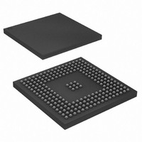
AT91SAM9260B-CU-999 Atmel, AT91SAM9260B-CU-999 Datasheet - Page 575

AT91SAM9260B-CU-999
Manufacturer Part Number
AT91SAM9260B-CU-999
Description
IC MCU ARM9 217LFBGA
Manufacturer
Atmel
Series
AT91SAMr
Datasheet
1.AT91SAM9260B-CU-999.pdf
(798 pages)
Specifications of AT91SAM9260B-CU-999
Core Processor
ARM9
Core Size
16/32-Bit
Speed
180MHz
Connectivity
EBI/EMI, Ethernet, I²C, MMC, SPI, SSC, UART/USART, USB
Peripherals
POR, WDT
Number Of I /o
96
Program Memory Size
32KB (32K x 8)
Program Memory Type
ROM
Ram Size
24K x 8
Voltage - Supply (vcc/vdd)
1.65 V ~ 1.95 V
Data Converters
A/D 4x10b
Oscillator Type
Internal
Operating Temperature
-40°C ~ 85°C
Package / Case
217-LFBGA
Processor Series
AT91SAMx
Core
ARM926EJ-S
Data Bus Width
32 bit
Data Ram Size
8 KB
Interface Type
2-Wire, EBI, I2S, SPI, USART
Maximum Clock Frequency
180 MHz
Number Of Programmable I/os
96
Number Of Timers
6
Maximum Operating Temperature
+ 85 C
Mounting Style
SMD/SMT
3rd Party Development Tools
JTRACE-ARM-2M, MDK-ARM, RL-ARM, ULINK2
Development Tools By Supplier
AT91SAM-ICE, AT91-ISP, AT91SAM9260-EK
Minimum Operating Temperature
- 40 C
On-chip Adc
10 bit, 4 Channel
For Use With
AT91SAM9260-EK - KIT EVAL FOR AT91SAM9260AT91SAM-ICE - EMULATOR FOR AT91 ARM7/ARM9
Lead Free Status / RoHS Status
Lead free / RoHS Compliant
Eeprom Size
-
Lead Free Status / Rohs Status
Details
Available stocks
Company
Part Number
Manufacturer
Quantity
Price
- Current page: 575 of 798
- Download datasheet (12Mb)
34.10.11 MCI Status Register
Name:
Access Type:
• CMDRDY: Command Ready
0 = A command is in progress.
1 = The last command has been sent. Cleared when writing in the MCI_CMDR.
• RXRDY: Receiver Ready
0 = Data has not yet been received since the last read of MCI_RDR.
1 = Data has been received since the last read of MCI_RDR.
• TXRDY: Transmit Ready
0= The last data written in MCI_TDR has not yet been transferred in the Shift Register.
1= The last data written in MCI_TDR has been transferred in the Shift Register.
• BLKE: Data Block Ended
This flag must be used only for Write Operations.
0 = A data block transfer is not yet finished. Cleared when reading the MCI_SR.
1 = A data block transfer has ended, including the CRC16 Status transmission.
In PDC mode (PDCMODE=1), the flag is set when the CRC Status of the last block has been transmitted (TXBUFE already
set).
Otherwise (PDCMODE=0), the flag is set for each transmitted CRC Status.
Refer to the MMC or SD Specification for more details concerning the CRC Status.
• DTIP: Data Transfer in Progress
0 = No data transfer in progress.
1 = The current data transfer is still in progress, including CRC16 calculation. Cleared at the end of the CRC16 calculation.
• NOTBUSY: MCI Not Busy
This flag must be used only for Write Operations.
A block write operation uses a simple busy signalling of the write operation duration on the data (DAT0) line: during a data
transfer block, if the card does not have a free data receive buffer, the card indicates this condition by pulling down the data
line (DAT0) to LOW. The card stops pulling down the data line as soon as at least one receive buffer for the defined data
transfer block length becomes free.
The NOTBUSY flag allows to deal with these different states.
0 = The MCI is not ready for new data transfer. Cleared at the end of the card response.
6221I–ATARM–17-Jul-09
TXBUFE
ENDTX
UNRE
31
23
15
–
7
RXBUFF
ENDRX
OVRE
DTOE
30
22
14
MCI_SR
Read-only
6
NOTBUSY
DCRCE
29
21
13
–
–
5
RTOE
DTIP
28
20
12
–
–
4
RENDE
BLKE
27
19
11
–
3
-
RCRCE
TXRDY
26
18
10
–
2
-
SDIOIRQB
AT91SAM9260
RXRDY
RDIRE
25
17
–
9
1
SDIOIRQA
CMDRDY
RINDE
24
16
–
8
0
575
Related parts for AT91SAM9260B-CU-999
Image
Part Number
Description
Manufacturer
Datasheet
Request
R

Part Number:
Description:
Manufacturer:
ATMEL Corporation
Datasheet:

Part Number:
Description:
KIT EVAL FOR AT91SAM9260
Manufacturer:
Atmel
Datasheet:

Part Number:
Description:
AT91 ARM Thumb Microcontrollers
Manufacturer:
ATMEL [ATMEL Corporation]
Datasheet:

Part Number:
Description:
AT91 ARM Thumb Microcontrollers
Manufacturer:
ATMEL Corporation
Datasheet:

Part Number:
Description:
At91 Arm Thumb Microcontrollers
Manufacturer:
ATMEL Corporation
Datasheet:

Part Number:
Description:
MCU, MPU & DSP Development Tools DEV BRD FOR AT91SAM9260
Manufacturer:
Olimex Ltd.
Datasheet:

Part Number:
Description:
MCU, MPU & DSP Development Tools KICKSTART KIT FOR AT91SAM9 PLUS
Manufacturer:
IAR Systems

Part Number:
Description:
DEV KIT FOR AVR/AVR32
Manufacturer:
Atmel
Datasheet:

Part Number:
Description:
INTERVAL AND WIPE/WASH WIPER CONTROL IC WITH DELAY
Manufacturer:
ATMEL Corporation
Datasheet:

Part Number:
Description:
Low-Voltage Voice-Switched IC for Hands-Free Operation
Manufacturer:
ATMEL Corporation
Datasheet:

Part Number:
Description:
MONOLITHIC INTEGRATED FEATUREPHONE CIRCUIT
Manufacturer:
ATMEL Corporation
Datasheet:

Part Number:
Description:
AM-FM Receiver IC U4255BM-M
Manufacturer:
ATMEL Corporation
Datasheet:

Part Number:
Description:
Monolithic Integrated Feature Phone Circuit
Manufacturer:
ATMEL Corporation
Datasheet:

Part Number:
Description:
Multistandard Video-IF and Quasi Parallel Sound Processing
Manufacturer:
ATMEL Corporation
Datasheet:


