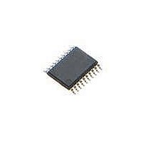
P89LPC972FDH,129 NXP Semiconductors, P89LPC972FDH,129 Datasheet - Page 30

P89LPC972FDH,129
Manufacturer Part Number
P89LPC972FDH,129
Description
MCU 80C51 8KB FLASH 20TSSOP
Manufacturer
NXP Semiconductors
Series
LPC900r
Datasheet
1.P89LPC970FDH129.pdf
(66 pages)
Specifications of P89LPC972FDH,129
Program Memory Type
FLASH
Program Memory Size
8KB (8K x 8)
Package / Case
20-TSSOP
Core Processor
8051
Core Size
8-Bit
Speed
18MHz
Connectivity
I²C, SPI, UART/USART
Peripherals
Brown-out Detect/Reset, POR, PWM, WDT
Number Of I /o
18
Ram Size
256 x 8
Voltage - Supply (vcc/vdd)
2.4 V ~ 5.5 V
Oscillator Type
Internal
Operating Temperature
-40°C ~ 85°C
Processor Series
P89LPC
Core
80C51
Data Bus Width
8 bit
Data Ram Size
256 B
Interface Type
I2C, SPI, UART
Maximum Clock Frequency
18 MHz
Number Of Programmable I/os
15
Number Of Timers
5
Operating Supply Voltage
2.4 V to 5.5 V
Maximum Operating Temperature
+ 85 C
Mounting Style
SMD/SMT
3rd Party Development Tools
PK51, CA51, A51, ULINK2
Minimum Operating Temperature
- 40 C
Lead Free Status / RoHS Status
Lead free / RoHS Compliant
Eeprom Size
-
Data Converters
-
Lead Free Status / Rohs Status
Lead free / RoHS Compliant
Other names
935290299129
NXP Semiconductors
P89LPC97X
Product data sheet
7.19.3.1 Mode 3
7.19.3.2 Mode 6
7.19.1 Mode 0
7.19.2 Mode 1
7.19.3 Mode 2
7.19.4 Timer overflow toggle output
7.20 Timers/counters 2, 3 and 4
In the ‘Counter’ function, the register is incremented in response to a 1-to-0 transition at its
corresponding count input pin, T0 or T1. In this function, the count input is sampled once
during every machine cycle.
Timer 0 and Timer 1 have five operating modes (Modes 0, 1, 2, 3 and 6). Modes 0, 1, 2
and 6 are the same for both Timers/Counters. Mode 3 is different.
Putting either Timer into Mode 0 makes it look like an 8048 Timer, which is an 8-bit
Counter with a divide-by-32 prescaler. In this mode, the Timer register is configured as a
13-bit register. Mode 0 operation is the same for Timer 0 and Timer 1.
Mode 1 is the same as Mode 0, except that all 16 bits of the timer register are used.
Mode 2 configures the Timer register as an 8-bit Counter with automatic reload. Mode 2
operation is the same for Timer 0 and Timer 1.
When Timer 1 is in Mode 3 it is stopped. Timer 0 in Mode 3 forms two separate 8-bit
counters and is provided for applications that require an extra 8-bit timer. When Timer 1 is
in Mode 3 it can still be used by the serial port as a baud rate generator.
In this mode, the corresponding timer can be changed to a PWM with a full period of
256 timer clocks.
Timers 0 and 1 can be configured to automatically toggle a port output whenever a timer
overflow occurs. The same device pins that are used for the T0 and T1 count inputs are
also used for the timer toggle outputs. The port outputs will be a logic 1 prior to the first
timer overflow when this mode is turned on.
The P89LPC970/971/972 has three external 16-bit timer/counters. All can be configured
to operate either as timers or event counters. An option to automatically toggle pin Tx (x =
2, 3 or 4) upon timer overflow has been added.
In the ‘Timer’ function, the register is incremented every PCLK.
In the ‘Counter’ function, the register is incremented in response to a 1-to-0 transition at its
corresponding count input pin (T2/T3 /T4). In this function, the count input is sampled
once during every machine cycle.
Only external Timer 2/3/4 has the external input pin TxEX (x = 2, 3 or 4). A 1-to-0
transition on this pin can trigger a reload or capture event.
Timer 2, Timer 3 and Timer 4 have three operating modes (Modes 0, 1 and 2).
All information provided in this document is subject to legal disclaimers.
Rev. 3 — 8 June 2010
8-bit microcontroller with accelerated two-clock 80C51 core
P89LPC970/971/972
© NXP B.V. 2010. All rights reserved.
30 of 66


