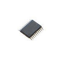
P89LPC972FDH,129 NXP Semiconductors, P89LPC972FDH,129 Datasheet - Page 43

P89LPC972FDH,129
Manufacturer Part Number
P89LPC972FDH,129
Description
MCU 80C51 8KB FLASH 20TSSOP
Manufacturer
NXP Semiconductors
Series
LPC900r
Datasheet
1.P89LPC970FDH129.pdf
(66 pages)
Specifications of P89LPC972FDH,129
Program Memory Type
FLASH
Program Memory Size
8KB (8K x 8)
Package / Case
20-TSSOP
Core Processor
8051
Core Size
8-Bit
Speed
18MHz
Connectivity
I²C, SPI, UART/USART
Peripherals
Brown-out Detect/Reset, POR, PWM, WDT
Number Of I /o
18
Ram Size
256 x 8
Voltage - Supply (vcc/vdd)
2.4 V ~ 5.5 V
Oscillator Type
Internal
Operating Temperature
-40°C ~ 85°C
Processor Series
P89LPC
Core
80C51
Data Bus Width
8 bit
Data Ram Size
256 B
Interface Type
I2C, SPI, UART
Maximum Clock Frequency
18 MHz
Number Of Programmable I/os
15
Number Of Timers
5
Operating Supply Voltage
2.4 V to 5.5 V
Maximum Operating Temperature
+ 85 C
Mounting Style
SMD/SMT
3rd Party Development Tools
PK51, CA51, A51, ULINK2
Minimum Operating Temperature
- 40 C
Lead Free Status / RoHS Status
Lead free / RoHS Compliant
Eeprom Size
-
Data Converters
-
Lead Free Status / Rohs Status
Lead free / RoHS Compliant
Other names
935290299129
NXP Semiconductors
P89LPC97X
Product data sheet
7.29.6 ICP
7.29.7 IAP
7.29.8 ISP
7.29.9 Power-on reset code execution
ICP is performed without removing the microcontroller from the system. The ICP facility
consists of internal hardware resources to facilitate remote programming of the
P89LPC970/971/972 through a two-wire serial interface. The NXP ICP facility has made
in-circuit programming in an embedded application - using commercially available
programmers - possible with a minimum of additional expense in components and circuit
board area. The ICP function uses five pins. Only a small connector needs to be available
to interface your application to a commercial programmer in order to use this feature.
Additional details may be found in the P89LPC970/971/972 User manual.
IAP is performed in the application under the control of the microcontroller’s firmware. The
IAP facility consists of internal hardware resources to facilitate programming and erasing.
The NXP IAP has made in-application programming in an embedded application possible
without additional components. Two methods are available to accomplish IAP. A set of
predefined IAP functions are provided in a Boot ROM and can be called through a
common interface, PGM_MTP. Several IAP calls are available for use by an application
program to permit selective erasing and programming of flash sectors, pages, security
bits, configuration bytes, and device ID. These functions are selected by setting up the
microcontroller’s registers before making a call to PGM_MTP at FF03H. The Boot ROM
occupies the program memory space at the top of the address space from FF00H to
FEFFH, thereby not conflicting with the user program memory space.
In addition, IAP operations can be accomplished through the use of four SFRs consisting
of a control/status register, a data register, and two address registers. Additional details
may be found in the P89LPC970/971/972 User manual.
ISP is performed without removing the microcontroller from the system. The ISP facility
consists of a series of internal hardware resources coupled with internal firmware to
facilitate remote programming of the P89LPC970/971/972 through the serial port. This
firmware is provided by NXP and embedded within each P89LPC970/971/972 device.
The NXP ISP facility has made in-system programming in an embedded application
possible with a minimum of additional expense in components and circuit board area. The
ISP function uses five pins (V
needs to be available to interface your application to an external circuit in order to use this
feature.
The P89LPC970/971/972 contains two special flash elements: the Boot Vector and the
Boot Status bit. Following reset, the P89LPC970/971/972 examines the contents of the
Boot Status bit. If the Boot Status bit is set to zero, power-up execution starts at location
0000H, which is the normal start address of the user’s application code. When the Boot
Status bit is set to a value other than zero, the contents of the Boot Vector are used as the
high byte of the execution address and the low byte is set to 00H.
Table 9
bootloader is pre-programmed into the address space indicated and uses the indicated
bootloader entry point to perform ISP functions. This code can be erased by the user.
shows the factory default Boot Vector setting for these devices. A factory-provided
All information provided in this document is subject to legal disclaimers.
Rev. 3 — 8 June 2010
8-bit microcontroller with accelerated two-clock 80C51 core
DD
, V
SS
, TXD, RXD, and RST). Only a small connector
P89LPC970/971/972
© NXP B.V. 2010. All rights reserved.
43 of 66


