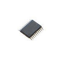
P89LPC972FDH,129 NXP Semiconductors, P89LPC972FDH,129 Datasheet - Page 36

P89LPC972FDH,129
Manufacturer Part Number
P89LPC972FDH,129
Description
MCU 80C51 8KB FLASH 20TSSOP
Manufacturer
NXP Semiconductors
Series
LPC900r
Datasheet
1.P89LPC970FDH129.pdf
(66 pages)
Specifications of P89LPC972FDH,129
Program Memory Type
FLASH
Program Memory Size
8KB (8K x 8)
Package / Case
20-TSSOP
Core Processor
8051
Core Size
8-Bit
Speed
18MHz
Connectivity
I²C, SPI, UART/USART
Peripherals
Brown-out Detect/Reset, POR, PWM, WDT
Number Of I /o
18
Ram Size
256 x 8
Voltage - Supply (vcc/vdd)
2.4 V ~ 5.5 V
Oscillator Type
Internal
Operating Temperature
-40°C ~ 85°C
Processor Series
P89LPC
Core
80C51
Data Bus Width
8 bit
Data Ram Size
256 B
Interface Type
I2C, SPI, UART
Maximum Clock Frequency
18 MHz
Number Of Programmable I/os
15
Number Of Timers
5
Operating Supply Voltage
2.4 V to 5.5 V
Maximum Operating Temperature
+ 85 C
Mounting Style
SMD/SMT
3rd Party Development Tools
PK51, CA51, A51, ULINK2
Minimum Operating Temperature
- 40 C
Lead Free Status / RoHS Status
Lead free / RoHS Compliant
Eeprom Size
-
Data Converters
-
Lead Free Status / Rohs Status
Lead free / RoHS Compliant
Other names
935290299129
NXP Semiconductors
P89LPC97X
Product data sheet
Fig 10. SPI block diagram
SPI STATUS REGISTER
BY 4, 16, 64, 128
CPU clock
DIVIDER
SELECT
SPI CONTROL
7.24 SPI (Pin remap)
The P89LPC970/971/972 provides another high-speed serial communication interface:
the SPI interface. SPI is a full-duplex, high-speed, synchronous communication bus with
two operation modes: Master mode and Slave mode. Up to 3 Mbit/s can be supported in
either Master mode or Slave mode. It has a Transfer Completion Flag and Write Collision
Flag Protection.
The SPI interface has four pins: SPICLK, MOSI, MISO and SS:
Typical connections are shown in
•
•
SPICLK, MOSI and MISO are typically tied together between two or more SPI
devices. Data flows from master to slave on MOSI (Master Out Slave In) pin and flows
from slave to master on MISO (Master In Slave Out) pin. The SPICLK signal is output
in the Master mode and is input in the Slave mode. If the SPI system is disabled, i.e.,
SPEN (SPCTL.6) = 0 (reset value), these pins are configured for port functions.
SS is the optional slave select pin. In a typical configuration, an SPI master asserts
one of its port pins to select one SPI device as the current slave. An SPI slave device
uses its SS pin to determine whether it is selected.
interrupt
request
SPI clock (master)
SPI
MSTR
SPEN
All information provided in this document is subject to legal disclaimers.
internal
data
Rev. 3 — 8 June 2010
bus
8-bit microcontroller with accelerated two-clock 80C51 core
SPI CONTROL REGISTER
8-BIT SHIFT REGISTER
READ DATA BUFFER
CLOCK LOGIC
Figure 11
clock
through
P89LPC970/971/972
Figure
13.
M
M
M
S
S
S
CONTROL
LOGIC
PIN
© NXP B.V. 2010. All rights reserved.
002aaf091
MISO
P1.6
MOSI
P1.7
SPICLK
P0.0
SS
P1.4
36 of 66


