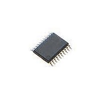
P89LPC972FDH,129 NXP Semiconductors, P89LPC972FDH,129 Datasheet - Page 32

P89LPC972FDH,129
Manufacturer Part Number
P89LPC972FDH,129
Description
MCU 80C51 8KB FLASH 20TSSOP
Manufacturer
NXP Semiconductors
Series
LPC900r
Datasheet
1.P89LPC970FDH129.pdf
(66 pages)
Specifications of P89LPC972FDH,129
Program Memory Type
FLASH
Program Memory Size
8KB (8K x 8)
Package / Case
20-TSSOP
Core Processor
8051
Core Size
8-Bit
Speed
18MHz
Connectivity
I²C, SPI, UART/USART
Peripherals
Brown-out Detect/Reset, POR, PWM, WDT
Number Of I /o
18
Ram Size
256 x 8
Voltage - Supply (vcc/vdd)
2.4 V ~ 5.5 V
Oscillator Type
Internal
Operating Temperature
-40°C ~ 85°C
Processor Series
P89LPC
Core
80C51
Data Bus Width
8 bit
Data Ram Size
256 B
Interface Type
I2C, SPI, UART
Maximum Clock Frequency
18 MHz
Number Of Programmable I/os
15
Number Of Timers
5
Operating Supply Voltage
2.4 V to 5.5 V
Maximum Operating Temperature
+ 85 C
Mounting Style
SMD/SMT
3rd Party Development Tools
PK51, CA51, A51, ULINK2
Minimum Operating Temperature
- 40 C
Lead Free Status / RoHS Status
Lead free / RoHS Compliant
Eeprom Size
-
Data Converters
-
Lead Free Status / Rohs Status
Lead free / RoHS Compliant
Other names
935290299129
NXP Semiconductors
P89LPC97X
Product data sheet
7.22.2 Mode 1
7.22.3 Mode 2
7.22.4 Mode 3
7.22.5 Baud rate generator and selection
7.22.6 Framing error
10 bits are transmitted (through TXD) or received (through RXD): a start bit (logic 0),
8 data bits (LSB first), and a stop bit (logic 1). When data is received, the stop bit is stored
in RB8 in special function register SCON. The baud rate is variable and is determined by
the Timer 1 overflow rate or the baud rate generator (described in
rate generator and
11 bits are transmitted (through TXD) or received (through RXD): start bit (logic 0), 8 data
bits (LSB first), a programmable 9
transmitted, the 9
Or, for example, the parity bit (P, in the PSW) could be moved into TB8. When data is
received, the 9
bit is not saved. The baud rate is programmable to either
frequency, as determined by the SMOD1 bit in PCON.
11 bits are transmitted (through TXD) or received (through RXD): a start bit (logic 0), 8
data bits (LSB first), a programmable 9
the same as Mode 2 in all respects except baud rate. The baud rate in Mode 3 is variable
and is determined by the Timer 1 overflow rate or the baud rate generator (described in
Section 7.22.5 “Baud rate generator and
The P89LPC970/971/972 enhanced UART has an independent baud rate generator. The
baud rate is determined by a baud-rate preprogrammed into the BRGR1 and BRGR0
SFRs which together form a 16-bit baud rate divisor value that works in a similar manner
as Timer 1 but is much more accurate. If the baud rate generator is used, Timer 1 can be
used for other timing functions.
The UART can use either Timer 1 or the baud rate generator output (see
that Timer T1 is further divided by 2 if the SMOD1 bit (PCON.7) is cleared. The
independent baud rate generators use OSCCLK.
Framing error is reported in the status register (SSTAT). In addition, if SMOD0 (PCON.6)
is logic 1, framing errors can be made available in SCON.7 respectively. If SMOD0 is
logic 0, SCON.7 is SM0. It is recommended that SM0 and SM1 (SCON.7:6) are set up
when SMOD0 is logic 0.
Fig 7.
baud rate generator
Baud rate sources for UART (Modes 1, 3)
timer 1 overflow
(CCLK-based)
(PCLK-based)
th
All information provided in this document is subject to legal disclaimers.
data bit goes into RB8 in special function register SCON, while the stop
th
selection”).
data bit (TB8 in SCON) can be assigned the value of logic 0 or logic 1.
Rev. 3 — 8 June 2010
8-bit microcontroller with accelerated two-clock 80C51 core
÷2
th
data bit, and a stop bit (logic 1). When data is
SMOD1 = 1
SMOD1 = 0
th
data bit, and a stop bit (logic 1). In fact, Mode 3 is
selection”).
P89LPC970/971/972
SBRGS = 0
SBRGS = 1
1
⁄
16
or
baud rate modes 1 and 3
1
⁄
32
Section 7.22.5 “Baud
of the CPU clock
© NXP B.V. 2010. All rights reserved.
Figure
002aaa897
7). Note
32 of 66


