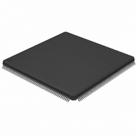
LPC2939FBD208,551 NXP Semiconductors, LPC2939FBD208,551 Datasheet - Page 28

LPC2939FBD208,551
Manufacturer Part Number
LPC2939FBD208,551
Description
IC ARM9 MCU FLASH 768KB 208-LQFP
Manufacturer
NXP Semiconductors
Series
LPC2900r
Datasheet
1.LPC2939FBD208551.pdf
(99 pages)
Specifications of LPC2939FBD208,551
Core Processor
ARM9
Core Size
32-Bit
Speed
125MHz
Connectivity
CAN, EBI/EMI, I²C, LIN, SPI, UART/USART, USB, USB OTG
Peripherals
DMA, POR, PWM, WDT
Number Of I /o
152
Program Memory Size
768KB (768K x 8)
Program Memory Type
FLASH
Eeprom Size
16K x 8
Ram Size
56K x 8
Voltage - Supply (vcc/vdd)
1.71 V ~ 3.6 V
Data Converters
A/D 24x10b
Oscillator Type
Internal
Operating Temperature
-40°C ~ 85°C
Package / Case
208-LQFP
Processor Series
LPC29
Core
ARM968E-S
3rd Party Development Tools
MDK-ARM, RL-ARM, ULINK2
Development Tools By Supplier
OM11027
Package
208LQFP
Device Core
ARM968E-S
Family Name
LPC2900
Operating Supply Voltage
1.8|3.3 V
Data Bus Width
16|32 Bit
Number Of Programmable I/os
160
Interface Type
CAN/I2C/LIN/QSPI/UART/USB
On-chip Adc
24-chx10-bit
Number Of Timers
6
For Use With
568-4787 - BOARD EVAL LPC2939
Lead Free Status / RoHS Status
Lead free / RoHS Compliant
Other names
935287113551
Available stocks
Company
Part Number
Manufacturer
Quantity
Price
Company:
Part Number:
LPC2939FBD208,551
Manufacturer:
NXP Semiconductors
Quantity:
10 000
NXP Semiconductors
LPC2939_3
Product data sheet
6.10.1 DMA support for peripherals
6.10 General Purpose DMA (GPDMA) controller
Usage of the idle/turn-around time (IDCY) is demonstrated In
are added between a read and a write cycle in the same external memory device.
Address pins on the device are shared with other functions. When connecting external
memories, check that the I/O pin is programmed for the correct function. Control of these
settings is handled by the SCU.
The GPDMA controller allows peripheral-to memory, memory-to-peripheral,
peripheral-to-peripheral, and memory-to-memory transactions. Each DMA stream
provides unidirectional serial DMA transfers for a single source and destination. For
example, a bidirectional port requires one stream for transmit and one for receives. The
source and destination areas can each be either a memory region or a peripheral, and
can be accessed through the same AHB master or one area by each master.
The GPDMA controls eight DMA channels with hardware prioritization. The DMA
controller interfaces to the system via two AHB bus masters, each with a full 32-bit data
bus width. DMA operations may be set up for 8-bit, 16-bit, and 32-bit data widths, and can
be either big-endian or little-endian. Incrementing or non-incrementing addressing for
source and destination are supported, as well as programmable DMA burst size. Scatter
or gather DMA is supported through the use of linked lists. This means that the source
and destination areas do not have to occupy contiguous areas of memory.
The GPDMA supports the following peripherals: SPI0/1/2 and UART0/1. The GPDMA can
access both embedded SRAM blocks (16 kB and 32 kB), both TCMs, external static
memory, and flash memory.
Fig 7.
CLK(SYS)
WE
CS
OE
D
A
WSTOEN = 2, WSTWEN = 4, WST1 = 6, WST2 = 4, IDCY = 5
Reading/writing external memory
All information provided in this document is subject to legal disclaimers.
WSTOEN
Rev. 03 — 7 April 2010
WST1
ARM9 microcontroller with CAN, LIN, and USB
IDCY
WSTWEN
Figure
WST2
7. Extra wait states
LPC2939
© NXP B.V. 2010. All rights reserved.
002aae706
28 of 99


