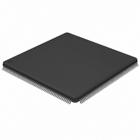
LPC2939FBD208,551 NXP Semiconductors, LPC2939FBD208,551 Datasheet - Page 50

LPC2939FBD208,551
Manufacturer Part Number
LPC2939FBD208,551
Description
IC ARM9 MCU FLASH 768KB 208-LQFP
Manufacturer
NXP Semiconductors
Series
LPC2900r
Datasheet
1.LPC2939FBD208551.pdf
(99 pages)
Specifications of LPC2939FBD208,551
Core Processor
ARM9
Core Size
32-Bit
Speed
125MHz
Connectivity
CAN, EBI/EMI, I²C, LIN, SPI, UART/USART, USB, USB OTG
Peripherals
DMA, POR, PWM, WDT
Number Of I /o
152
Program Memory Size
768KB (768K x 8)
Program Memory Type
FLASH
Eeprom Size
16K x 8
Ram Size
56K x 8
Voltage - Supply (vcc/vdd)
1.71 V ~ 3.6 V
Data Converters
A/D 24x10b
Oscillator Type
Internal
Operating Temperature
-40°C ~ 85°C
Package / Case
208-LQFP
Processor Series
LPC29
Core
ARM968E-S
3rd Party Development Tools
MDK-ARM, RL-ARM, ULINK2
Development Tools By Supplier
OM11027
Package
208LQFP
Device Core
ARM968E-S
Family Name
LPC2900
Operating Supply Voltage
1.8|3.3 V
Data Bus Width
16|32 Bit
Number Of Programmable I/os
160
Interface Type
CAN/I2C/LIN/QSPI/UART/USB
On-chip Adc
24-chx10-bit
Number Of Timers
6
For Use With
568-4787 - BOARD EVAL LPC2939
Lead Free Status / RoHS Status
Lead free / RoHS Compliant
Other names
935287113551
Available stocks
Company
Part Number
Manufacturer
Quantity
Price
Company:
Part Number:
LPC2939FBD208,551
Manufacturer:
NXP Semiconductors
Quantity:
10 000
NXP Semiconductors
LPC2939_3
Product data sheet
6.15.7.1 Pin description
6.15.7.2 Clock description
6.16 Power, Clock and Reset control SubSystem (PCRSS)
The QEI module in the MSCSS has the following pins. These are combined with other
functions on the port pins of the LPC2939.
Table 26.
The QEI module is clocked by CLK_MSCSS_QEI, see
this clock is identical to CLK_MSCSS_APB since they are derived from the same base
clock BASE_MSCSS_CLK.
If the QEI is not used its CLK_MSCSS_QEI branch clock can be switched off.
The Power, Clock and Reset Control Subsystem in the LPC2939 includes a Clock
Generator Unit (CGU), a Reset Generator Unit (RGU), and a Power Management Unit
(PMU).
Figure 11
communication with the AHB system bus.
Symbol
QEI0 IDX
QEI0 PHA
QEI0 PHB
provides an overview of the PCRSS. An AHB-to-DTL bridge controls the
QEI pins
All information provided in this document is subject to legal disclaimers.
Pin name
IDX0
PHA0
PHB0
Rev. 03 — 7 April 2010
Direction
IN
IN
IN
ARM9 microcontroller with CAN, LIN, and USB
Table 26
Description
Index signal. Can be used to reset the position.
Sensor signal. Corresponds to PHA in
quadrature mode and to direction in
clock/direction mode.
Sensor signal. Corresponds to PHB in
quadrature mode and to clock signal in
clock/direction mode.
shows the QEI pins.
Section
6.7.2. The frequency of
LPC2939
© NXP B.V. 2010. All rights reserved.
50 of 99


