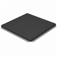
LPC2939FBD208,551 NXP Semiconductors, LPC2939FBD208,551 Datasheet - Page 54

LPC2939FBD208,551
Manufacturer Part Number
LPC2939FBD208,551
Description
IC ARM9 MCU FLASH 768KB 208-LQFP
Manufacturer
NXP Semiconductors
Series
LPC2900r
Datasheet
1.LPC2939FBD208551.pdf
(99 pages)
Specifications of LPC2939FBD208,551
Core Processor
ARM9
Core Size
32-Bit
Speed
125MHz
Connectivity
CAN, EBI/EMI, I²C, LIN, SPI, UART/USART, USB, USB OTG
Peripherals
DMA, POR, PWM, WDT
Number Of I /o
152
Program Memory Size
768KB (768K x 8)
Program Memory Type
FLASH
Eeprom Size
16K x 8
Ram Size
56K x 8
Voltage - Supply (vcc/vdd)
1.71 V ~ 3.6 V
Data Converters
A/D 24x10b
Oscillator Type
Internal
Operating Temperature
-40°C ~ 85°C
Package / Case
208-LQFP
Processor Series
LPC29
Core
ARM968E-S
3rd Party Development Tools
MDK-ARM, RL-ARM, ULINK2
Development Tools By Supplier
OM11027
Package
208LQFP
Device Core
ARM968E-S
Family Name
LPC2900
Operating Supply Voltage
1.8|3.3 V
Data Bus Width
16|32 Bit
Number Of Programmable I/os
160
Interface Type
CAN/I2C/LIN/QSPI/UART/USB
On-chip Adc
24-chx10-bit
Number Of Timers
6
For Use With
568-4787 - BOARD EVAL LPC2939
Lead Free Status / RoHS Status
Lead free / RoHS Compliant
Other names
935287113551
Available stocks
Company
Part Number
Manufacturer
Quantity
Price
Company:
Part Number:
LPC2939FBD208,551
Manufacturer:
NXP Semiconductors
Quantity:
10 000
NXP Semiconductors
LPC2939_3
Product data sheet
Configuration of the CGU0:
choice can be made from the primary and secondary clock generators according to
Figure
Any output generator (except for BASE_SAFE_CLK and BASE_PCR_CLK) can be
connected to either a fractional divider (FDIV0:6) or to one of the outputs of the PLL or to
LP_OSC/crystal oscillator directly. BASE_SAFE_CLK and BASE_PCR_CLK can use only
LP_OSC as source.
The fractional dividers can be connected to one of the outputs of the PLL or directly to
LP_OSC/crystal Oscillator.
The PLL is connected to the crystal oscillator.
In this way every output generating the base clocks can be configured to get the required
clock. Multiple output generators can be connected to the same primary or secondary
clock source, and multiple secondary clock sources can be connected to the same PLL
output or primary clock source.
Invalid selections/programming - connecting the PLL to an FDIV or to one of the PLL
outputs itself for example - will be blocked by hardware. The control register will not be
written, the previous value will be kept, although all other fields will be written with new
data. This prevents clocks being blocked by incorrect programming.
Default Clock Sources:
connected to LP_OSC at reset. In this way the device runs at a low frequency after reset.
It is recommended to switch BASE_SYS_CLK to a high-frequency clock generator as
(one of) the first step(s) in the boot code after verifying that the high-frequency clock
generator is running.
Clock Activity Detection:
and values of ‘CLK_SEL’ that would select those clocks are masked and not written to the
control registers. This is accomplished by adding a clock detector to every clock
Fig 13. Structure of the clock generation scheme
13.
OSCILLATOR
EXTERNAL
All information provided in this document is subject to legal disclaimers.
LP_OSC
Rev. 03 — 7 April 2010
Every secondary clock generator or output generator is
Clocks that are inactive are automatically regarded as invalid,
For every output generator generating the base clocks a
PLL
ARM9 microcontroller with CAN, LIN, and USB
clkout
clkout120
clkout240
CONTROL
OUTPUT
outputs
clock
LPC2939
© NXP B.V. 2010. All rights reserved.
FDIV0:6
002aad834
54 of 99


