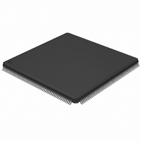
LPC2939FBD208,551 NXP Semiconductors, LPC2939FBD208,551 Datasheet - Page 43

LPC2939FBD208,551
Manufacturer Part Number
LPC2939FBD208,551
Description
IC ARM9 MCU FLASH 768KB 208-LQFP
Manufacturer
NXP Semiconductors
Series
LPC2900r
Datasheet
1.LPC2939FBD208551.pdf
(99 pages)
Specifications of LPC2939FBD208,551
Core Processor
ARM9
Core Size
32-Bit
Speed
125MHz
Connectivity
CAN, EBI/EMI, I²C, LIN, SPI, UART/USART, USB, USB OTG
Peripherals
DMA, POR, PWM, WDT
Number Of I /o
152
Program Memory Size
768KB (768K x 8)
Program Memory Type
FLASH
Eeprom Size
16K x 8
Ram Size
56K x 8
Voltage - Supply (vcc/vdd)
1.71 V ~ 3.6 V
Data Converters
A/D 24x10b
Oscillator Type
Internal
Operating Temperature
-40°C ~ 85°C
Package / Case
208-LQFP
Processor Series
LPC29
Core
ARM968E-S
3rd Party Development Tools
MDK-ARM, RL-ARM, ULINK2
Development Tools By Supplier
OM11027
Package
208LQFP
Device Core
ARM968E-S
Family Name
LPC2900
Operating Supply Voltage
1.8|3.3 V
Data Bus Width
16|32 Bit
Number Of Programmable I/os
160
Interface Type
CAN/I2C/LIN/QSPI/UART/USB
On-chip Adc
24-chx10-bit
Number Of Timers
6
For Use With
568-4787 - BOARD EVAL LPC2939
Lead Free Status / RoHS Status
Lead free / RoHS Compliant
Other names
935287113551
Available stocks
Company
Part Number
Manufacturer
Quantity
Price
Company:
Part Number:
LPC2939FBD208,551
Manufacturer:
NXP Semiconductors
Quantity:
10 000
NXP Semiconductors
LPC2939_3
Product data sheet
6.15.2 Pin description
6.15.3 Clock description
6.15.4 Analog-to-digital converter
The pins of the LPC2939 MSCSS associated with the three ADC modules are described
in
Section
Section
Section
The MSCSS is clocked from a number of different sources:
Each ADC has two clock areas; a APB part clocked by CLK_MSCSS_ADCx_APB (x = 0,
1, or 2) and a control part for the analog section clocked by CLK_ADCx = 0, 1, or 2), see
Section
All clocks are derived from the BASE_MSCSS_CLK, except for CLK_SYS_MSCSS_A
which is derived form BASE_SYS_CLK, and the CLK_ADCx clocks which are derived
from BASE_CLK_ADC. If specific PWM or ADC modules are not used their corresponding
clocks can be switched off.
The MSCSS in the LPC2939 includes three 10-bit successive-approximation
analog-to-digital converters.
The key features of the ADC interface module are:
•
•
•
•
•
•
•
•
•
•
•
•
•
•
Section
CLK_SYS_MSCSS_A clocks the AHB side of the AHB-to-APB bus bridge
CLK_MSCSS_APB clocks the subsystem APB bus
CLK_MSCSS_MTMR0/1 clocks the timers
CLK_MSCSS_PWM0:3 clocks the PWMs
ADC0: Eight analog inputs; time-multiplexed; measurement range up to 5.0 V
ADC1 and ADC2: Eight analog inputs; time-multiplexed; measurement range up to
3.3 V
External reference-level inputs
400 ksamples/s at 10-bit resolution up to 1500 ksamples/s at 2-bit resolution
Programmable resolution from 2-bit to10-bit
Single analog-to-digital conversion scan mode and continuous analog-to-digital
conversion scan mode
Optional conversion on transition on external start input, timer capture/match signal,
PWM_sync or ‘previous’ ADC
Converted digital values are stored in a register for each channel
Optional compare condition to generate a ‘less than’ or an ‘equal to or greater than’
compare-value indication for each channel
Power-down mode
6.15.5.4, pins directly connected to the MSCSS timer 1 module are described in
6.15.6.1, and pins connected to the quadrature encoder interface are described in
6.15.7.1.
6.7.2.
6.15.4.2. Pins connected to the four PWM modules are described in
All information provided in this document is subject to legal disclaimers.
Rev. 03 — 7 April 2010
ARM9 microcontroller with CAN, LIN, and USB
LPC2939
© NXP B.V. 2010. All rights reserved.
43 of 99


