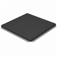
LPC2939FBD208,551 NXP Semiconductors, LPC2939FBD208,551 Datasheet - Page 52

LPC2939FBD208,551
Manufacturer Part Number
LPC2939FBD208,551
Description
IC ARM9 MCU FLASH 768KB 208-LQFP
Manufacturer
NXP Semiconductors
Series
LPC2900r
Datasheet
1.LPC2939FBD208551.pdf
(99 pages)
Specifications of LPC2939FBD208,551
Core Processor
ARM9
Core Size
32-Bit
Speed
125MHz
Connectivity
CAN, EBI/EMI, I²C, LIN, SPI, UART/USART, USB, USB OTG
Peripherals
DMA, POR, PWM, WDT
Number Of I /o
152
Program Memory Size
768KB (768K x 8)
Program Memory Type
FLASH
Eeprom Size
16K x 8
Ram Size
56K x 8
Voltage - Supply (vcc/vdd)
1.71 V ~ 3.6 V
Data Converters
A/D 24x10b
Oscillator Type
Internal
Operating Temperature
-40°C ~ 85°C
Package / Case
208-LQFP
Processor Series
LPC29
Core
ARM968E-S
3rd Party Development Tools
MDK-ARM, RL-ARM, ULINK2
Development Tools By Supplier
OM11027
Package
208LQFP
Device Core
ARM968E-S
Family Name
LPC2900
Operating Supply Voltage
1.8|3.3 V
Data Bus Width
16|32 Bit
Number Of Programmable I/os
160
Interface Type
CAN/I2C/LIN/QSPI/UART/USB
On-chip Adc
24-chx10-bit
Number Of Timers
6
For Use With
568-4787 - BOARD EVAL LPC2939
Lead Free Status / RoHS Status
Lead free / RoHS Compliant
Other names
935287113551
Available stocks
Company
Part Number
Manufacturer
Quantity
Price
Company:
Part Number:
LPC2939FBD208,551
Manufacturer:
NXP Semiconductors
Quantity:
10 000
NXP Semiconductors
LPC2939_3
Product data sheet
6.16.2.1 Functional description
6.16.2 Clock Generation Unit (CGU0)
The key features are:
Remark: Any clock-frequency adjustment has a direct impact on the timing of all on-board
peripherals.
The clock generation unit provides 10 internal clock sources as described in
Table 27.
[1]
[2]
For generation of these base clocks, the CGU consists of primary and secondary clock
generators and one output generator for each base clock.
Number
0
1
2
3
4
5
6
7
8
9
10
11
•
•
•
•
•
•
•
•
•
•
Generation of 11 base clocks selectable from several embedded clock sources
Crystal oscillator with power-down
Control PLL with power-down
Very low-power ring oscillator, always on to provide a safe clock
Seven fractional clock dividers with L/D division
Individual source selector for each base clock, with glitch-free switching
Autonomous clock-activity detection on every clock source
Protection against switching to invalid or inactive clock sources
Embedded frequency counter
Register write-protection mechanism to prevent unintentional alteration of clocks
Maximum frequency that guarantees stable operation of the LPC2939.
Fixed to low-power oscillator.
CGU0 base clocks
Name
BASE_SAFE_CLK
BASE_SYS_CLK
BASE_PCR_CLK
BASE_IVNSS_CLK
BASE_MSCSS_CLK
BASE_ICLK0_CLK
BASE_UART_CLK
BASE_SPI_CLK
BASE_TMR_CLK
BASE_ADC_CLK
reserved
BASE_ICLK1_CLK
All information provided in this document is subject to legal disclaimers.
Rev. 03 — 7 April 2010
Frequency
(MHz)
0.4
125
0.4
125
125
125
125
50
125
4.5
-
125
ARM9 microcontroller with CAN, LIN, and USB
[2]
[1]
Description
base safe clock (always on)
base system clock
base PCR subsystem clock
base IVNSS subsystem clock
base MSCSS subsystem clock
base internal clock 0, for CGU1
base UART clock
base SPI clock
base timers clock
base ADCs clock
-
base internal clock 1, for CGU1
LPC2939
© NXP B.V. 2010. All rights reserved.
Table
27.
52 of 99


