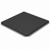
LPC2939FBD208,551 NXP Semiconductors, LPC2939FBD208,551 Datasheet - Page 35

LPC2939FBD208,551
Manufacturer Part Number
LPC2939FBD208,551
Description
IC ARM9 MCU FLASH 768KB 208-LQFP
Manufacturer
NXP Semiconductors
Series
LPC2900r
Datasheet
1.LPC2939FBD208551.pdf
(99 pages)
Specifications of LPC2939FBD208,551
Core Processor
ARM9
Core Size
32-Bit
Speed
125MHz
Connectivity
CAN, EBI/EMI, I²C, LIN, SPI, UART/USART, USB, USB OTG
Peripherals
DMA, POR, PWM, WDT
Number Of I /o
152
Program Memory Size
768KB (768K x 8)
Program Memory Type
FLASH
Eeprom Size
16K x 8
Ram Size
56K x 8
Voltage - Supply (vcc/vdd)
1.71 V ~ 3.6 V
Data Converters
A/D 24x10b
Oscillator Type
Internal
Operating Temperature
-40°C ~ 85°C
Package / Case
208-LQFP
Processor Series
LPC29
Core
ARM968E-S
3rd Party Development Tools
MDK-ARM, RL-ARM, ULINK2
Development Tools By Supplier
OM11027
Package
208LQFP
Device Core
ARM968E-S
Family Name
LPC2900
Operating Supply Voltage
1.8|3.3 V
Data Bus Width
16|32 Bit
Number Of Programmable I/os
160
Interface Type
CAN/I2C/LIN/QSPI/UART/USB
On-chip Adc
24-chx10-bit
Number Of Timers
6
For Use With
568-4787 - BOARD EVAL LPC2939
Lead Free Status / RoHS Status
Lead free / RoHS Compliant
Other names
935287113551
Available stocks
Company
Part Number
Manufacturer
Quantity
Price
Company:
Part Number:
LPC2939FBD208,551
Manufacturer:
NXP Semiconductors
Quantity:
10 000
NXP Semiconductors
LPC2939_3
Product data sheet
6.13.3.2 Clock description
6.13.4.1 Pin description
6.13.4 UARTs
The timer modules are clocked by two different clocks; CLK_SYS_PESS and CLK_TMRx
(x = 0 to 3), see
for power management. The frequency of all these clocks is identical as they are derived
from the same base clock BASE_CLK_TMR. The register interface towards the system
bus is clocked by CLK_SYS_PESS. The timer and prescale counters are clocked by
CLK_TMRx.
The LPC2939 contains two identical UARTs located at different peripheral base
addresses. The key features are:
The UART is commonly used to implement a serial interface such as RS232. The
LPC2939 contains two industry-standard 550 UARTs with 16-byte transmit and receive
FIFOs, but they can also be put into 450 mode without FIFOs.
Remark: The LIN controller can be configured to provide two additional standard UART
interfaces (see
The UART pins are combined with other functions on the port pins of the LPC2939.
Table 17
Table 17.
Symbol
UARTx TXD
UARTx RXD
UARTx CTS
UARTx DCD
UARTx DSR
UARTx DTR
UARTx RI
UARTx RTS
UARTx OUT1
UARTx OUT2
•
•
•
•
•
•
16-byte receive and transmit FIFOs
Register locations conform to 550 industry standard
Receiver FIFO trigger points at 1 byte, 4 bytes, 8 bytes and 14 bytes
Built-in baud rate generator
Support for RS-485/9-bit mode allows both software address detection and automatic
address detection using 9-bit mode
Both UARTs equipped with standard modem interface signals. This module also
provides full support for hardware flow control (auto-CTS/RTS)
shows the UART pins (x runs from 0 to 1).
UART pins
Section
All information provided in this document is subject to legal disclaimers.
Section
Pin name
TXDx
RXDx
CTSx
DCDx
DSRx
DTRx
RIx
RTSx
UxOUT1
UxOUT2
6.14.2).
Rev. 03 — 7 April 2010
6.7.2. Note that each timer has its own CLK_TMRx branch clock
Direction
OUT
IN
IN
IN
IN
OUT
IN
OUT
OUT
OUT
ARM9 microcontroller with CAN, LIN, and USB
Description
UART channel x transmit data output
UART channel x receive data input
UART channel x Clear To Send (modem)
UART channel x Data Carrier Detect (modem)
UART channel x Data Set Ready (modem)
UART channel x Data Terminal Ready
(modem)
UART Ring Indicator (modem)
UART Request To Send (modem)
UART channel x user designated output 1
UART channel x user designated output 2
LPC2939
© NXP B.V. 2010. All rights reserved.
35 of 99


