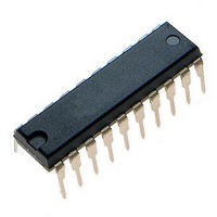
MCHC705JJ7CPE Freescale Semiconductor, MCHC705JJ7CPE Datasheet - Page 26

MCHC705JJ7CPE
Manufacturer Part Number
MCHC705JJ7CPE
Description
IC MCU 8BIT 224 BYTES RAM 20PDIP
Manufacturer
Freescale Semiconductor
Series
HC05r
Datasheet
1.MC705JJ7CDWE.pdf
(164 pages)
Specifications of MCHC705JJ7CPE
Core Processor
HC05
Core Size
8-Bit
Speed
2.1MHz
Connectivity
SIO
Peripherals
POR, Temp Sensor, WDT
Number Of I /o
14
Program Memory Size
6KB (6K x 8)
Program Memory Type
OTP
Ram Size
224 x 8
Voltage - Supply (vcc/vdd)
2.7 V ~ 5.5 V
Data Converters
A/D 4x12b
Oscillator Type
Internal
Operating Temperature
-40°C ~ 85°C
Package / Case
20-DIP (0.300", 7.62mm)
Processor Series
HC705JJ
Core
HC05
Data Bus Width
8 bit
Data Ram Size
224 B
Interface Type
SIOP
Maximum Clock Frequency
2.1 MHz
Number Of Programmable I/os
14
Number Of Timers
2
Maximum Operating Temperature
+ 85 C
Mounting Style
Through Hole
Minimum Operating Temperature
- 40 C
On-chip Adc
12 bit, 4 Channel
Package
20PDIP
Family Name
HC05
Maximum Speed
2.1 MHz
Operating Supply Voltage
3.3|5 V
Lead Free Status / RoHS Status
Lead free / RoHS Compliant
Eeprom Size
-
Lead Free Status / Rohs Status
Details
- Current page: 26 of 164
- Download datasheet (2Mb)
Memory
2.4 User and Interrupt Vector Mapping
The interrupt vectors are contained in the upper memory addresses above $1FF0 as shown in
2.5 Random-Access Memory (RAM)
The 224 addresses from $0020 to $00FF serve as both the user RAM and the stack RAM. The central
processor unit (CPU) uses five RAM bytes to save all CPU register contents before processing an
interrupt. During a subroutine call, the CPU uses two bytes to store the return address. The stack pointer
decrements during pushes and increments during pulls.
2.6 Erasable Programmable Read-Only Memory (EPROM)
The EPROM is located in three areas of the memory map:
26
•
•
•
Addresses $0700–$1EFF contain 6144 bytes of user EPROM.
Addresses $1FF0–$1FF1 contain 2 bytes of EPROM reserved for user vectors and COP and
security register (COPR), and the mask option register. Only bit 7 of $1FF0 is a programmable bit.
Addresses $1FF2–$1FFF contain 14 bytes of interrupt vectors.
Be careful when using nested subroutines or multiple interrupt levels. The
CPU may overwrite data in the RAM during a subroutine or during the
interrupt stacking operation.
MC68HC705JJ7 • MC68HC705JP7 Advance Information Data Sheet, Rev. 4.1
Address
$1FFA
$1FFB
$1FFC
$1FFD
$1FFE
$1FFF
$1FF0
$1FF1
$1FF2
$1FF3
$1FF4
$1FF5
$1FF6
$1FF7
$1FF8
$1FF9
Figure 2-4. Vector Mapping
COP Register and EPROM Security
Core Timer Interrupt Vector (MSB)
Core Timer Interrupt Vector (LSB)
Analog Interrupt Vector (MSB)
Analog Interrupt Vector (LSB)
Serial Interrupt Vector ((LSB)
Serial Interrupt Vector (MSB)
Timer Interrupt Vector (MSB)
Timer Interrupt Vector (LSB)
External IRQ Vector (MSB)
External IRQ Vector (LSB)
NOTE
Mask Option Register
Reset Vector (MSB)
Register Name
Reset Vector (LSB)
SWI Vector (MSB)
SWI Vector (LSB)
Freescale Semiconductor
Figure
2-4.
Related parts for MCHC705JJ7CPE
Image
Part Number
Description
Manufacturer
Datasheet
Request
R
Part Number:
Description:
Manufacturer:
Freescale Semiconductor, Inc
Datasheet:
Part Number:
Description:
Manufacturer:
Freescale Semiconductor, Inc
Datasheet:
Part Number:
Description:
Manufacturer:
Freescale Semiconductor, Inc
Datasheet:
Part Number:
Description:
Manufacturer:
Freescale Semiconductor, Inc
Datasheet:
Part Number:
Description:
Manufacturer:
Freescale Semiconductor, Inc
Datasheet:
Part Number:
Description:
Manufacturer:
Freescale Semiconductor, Inc
Datasheet:
Part Number:
Description:
Manufacturer:
Freescale Semiconductor, Inc
Datasheet:
Part Number:
Description:
Manufacturer:
Freescale Semiconductor, Inc
Datasheet:
Part Number:
Description:
Manufacturer:
Freescale Semiconductor, Inc
Datasheet:
Part Number:
Description:
Manufacturer:
Freescale Semiconductor, Inc
Datasheet:
Part Number:
Description:
Manufacturer:
Freescale Semiconductor, Inc
Datasheet:
Part Number:
Description:
Manufacturer:
Freescale Semiconductor, Inc
Datasheet:
Part Number:
Description:
Manufacturer:
Freescale Semiconductor, Inc
Datasheet:
Part Number:
Description:
Manufacturer:
Freescale Semiconductor, Inc
Datasheet:
Part Number:
Description:
Manufacturer:
Freescale Semiconductor, Inc
Datasheet:


