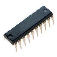
MCHC705JJ7CPE Freescale Semiconductor, MCHC705JJ7CPE Datasheet - Page 97

MCHC705JJ7CPE
Manufacturer Part Number
MCHC705JJ7CPE
Description
IC MCU 8BIT 224 BYTES RAM 20PDIP
Manufacturer
Freescale Semiconductor
Series
HC05r
Datasheet
1.MC705JJ7CDWE.pdf
(164 pages)
Specifications of MCHC705JJ7CPE
Core Processor
HC05
Core Size
8-Bit
Speed
2.1MHz
Connectivity
SIO
Peripherals
POR, Temp Sensor, WDT
Number Of I /o
14
Program Memory Size
6KB (6K x 8)
Program Memory Type
OTP
Ram Size
224 x 8
Voltage - Supply (vcc/vdd)
2.7 V ~ 5.5 V
Data Converters
A/D 4x12b
Oscillator Type
Internal
Operating Temperature
-40°C ~ 85°C
Package / Case
20-DIP (0.300", 7.62mm)
Processor Series
HC705JJ
Core
HC05
Data Bus Width
8 bit
Data Ram Size
224 B
Interface Type
SIOP
Maximum Clock Frequency
2.1 MHz
Number Of Programmable I/os
14
Number Of Timers
2
Maximum Operating Temperature
+ 85 C
Mounting Style
Through Hole
Minimum Operating Temperature
- 40 C
On-chip Adc
12 bit, 4 Channel
Package
20PDIP
Family Name
HC05
Maximum Speed
2.1 MHz
Operating Supply Voltage
3.3|5 V
Lead Free Status / RoHS Status
Lead free / RoHS Compliant
Eeprom Size
-
Lead Free Status / Rohs Status
Details
9.2.2 Serial Data Input (SDI)
The SDI pin becomes an input as soon as the SIOP subsystem is enabled. New data is presented to the
SDI pin on the falling edge of SCK. Valid data must be present at least 100 nanoseconds before the rising
edge of SCK and remain valid for 100 nanoseconds after the rising edge of SCK. See
9.2.3 Serial Data Output (SDO)
The SDO pin becomes an output as soon as the SIOP subsystem is enabled. The state of the PB5/SDO
pin reflects the value of the first bit received on the previous transmission. Prior to enabling the SIOP, the
PB5/SDO can be initialized to determine the beginning state. While SIOP is enabled, the port B logic
cannot be used as a standard output since that pin is connected to the last stage of the SIOP serial shift
register. A control bit (LSBF) is included in the SCR to allow the data to be transmitted in either the MSB
first format or the LSB first format.
The first data bit will be shifted out to the SDO pin on the first falling edge of the SCK. The remaining data
bits will be shifted out to the SDI pin on subsequent falling edges of SCK. The SDO pin will present valid
data at least 100 nanoseconds before the rising edge of the SCK and remain valid for 100 nanoseconds
after the rising edge of SCK. See
9.3 SIOP Registers
The SIOP is programmed and controlled by the SIOP control register (SCR) located at address $000A,
the SIOP status register (SSR) located at address $000B, and the SIOP data register (SDR) located at
address $000C.
9.3.1 SIOP Control Register (SCR)
The SIOP control register (SCR) is located at address $000A and contains seven control bits and a
write-only reset of the interrupt flag.
the value of each bit after reset.
SPIE — Serial Peripheral Interrupt Enable Bit
Freescale Semiconductor
The SPIE bit enables the SIOP to generate an interrupt whenever the SPIF flag bit in the SSR is set.
Clearing the SPIE bit will not affect the state of the SPIF flag bit and will not terminate a serial interrupt
once the interrupt sequence has started. Reset clears the SPIE bit.
1 = Serial interrupt enabled
0 = Serial interrupt disabled
Address:
If the SPIE bit is cleared just after the serial interrupt sequence has started
(for instance, the CPU status is being stacked), then the CPU will be unable
Reset:
Read:
Write:
MC68HC705JJ7 • MC68HC705JP7 Advance Information Data Sheet, Rev. 4.1
$000A
SPIE
Bit 7
0
Figure 9-4. SIOP Control Register (SCR)
SPE
Figure
6
0
Figure 9-4
9-3.
LSBF
5
0
shows the position of each bit in the register and indicates
NOTE
MSTR
4
0
SPIR
3
0
0
CPHA
2
0
SPR1
1
0
SPR0
Figure
Bit 0
0
SIOP Registers
9-3.
97


