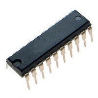
MCHC705JJ7CPE Freescale Semiconductor, MCHC705JJ7CPE Datasheet - Page 94

MCHC705JJ7CPE
Manufacturer Part Number
MCHC705JJ7CPE
Description
IC MCU 8BIT 224 BYTES RAM 20PDIP
Manufacturer
Freescale Semiconductor
Series
HC05r
Datasheet
1.MC705JJ7CDWE.pdf
(164 pages)
Specifications of MCHC705JJ7CPE
Core Processor
HC05
Core Size
8-Bit
Speed
2.1MHz
Connectivity
SIO
Peripherals
POR, Temp Sensor, WDT
Number Of I /o
14
Program Memory Size
6KB (6K x 8)
Program Memory Type
OTP
Ram Size
224 x 8
Voltage - Supply (vcc/vdd)
2.7 V ~ 5.5 V
Data Converters
A/D 4x12b
Oscillator Type
Internal
Operating Temperature
-40°C ~ 85°C
Package / Case
20-DIP (0.300", 7.62mm)
Processor Series
HC705JJ
Core
HC05
Data Bus Width
8 bit
Data Ram Size
224 B
Interface Type
SIOP
Maximum Clock Frequency
2.1 MHz
Number Of Programmable I/os
14
Number Of Timers
2
Maximum Operating Temperature
+ 85 C
Mounting Style
Through Hole
Minimum Operating Temperature
- 40 C
On-chip Adc
12 bit, 4 Channel
Package
20PDIP
Family Name
HC05
Maximum Speed
2.1 MHz
Operating Supply Voltage
3.3|5 V
Lead Free Status / RoHS Status
Lead free / RoHS Compliant
Eeprom Size
-
Lead Free Status / Rohs Status
Details
Analog Subsystem
8.11 Port B Interaction with Analog Inputs
The analog subsystem is connected directly to the port B I/O pins without any intervening gates. It is,
therefore, possible to measure the voltages on port B pins set as inputs or to have the analog voltage
measurements corrupted by port B pins set as outputs.
8.12 Port B Pins as Inputs
All the port B pins will power up as inputs or return to inputs after a reset of the device since the bits in the
port B data direction register will be reset.
If any port B pins are to be used for analog voltage measurements, they should be left as inputs. In this
case, not only can the voltage on the pin be measured, but the logic state of the port B pins can be read
from location $0002.
8.13 Port B Pulldowns
All the port B pins have internal software programmable pulldown devices available dependent on the
state of the SWPDI bit in the mask option register (MOR).
If the pulldowns are enabled, they will create an approximate 100 µA load to any analog source connected
to the pin. In some cases, the analog source may be able to supply this current without causing any error
due to the analog source output impedance. Since this may not always be true, it is therefore best to
disable port B pulldowns on those pins used for analog input sources.
8.14 Noise Sensitivity
In addition to the normal effects of electrical noise on the analog input signal there can also be other
noise-related effects caused by the digital-to-analog interface. Since there is only one V
return for both
SS
the digital and the analog subsystems on the device, currents in the digital section may affect the analog
ground reference within the device. This can add voltage offsets to measured inputs or cause
channel-to-channel crosstalk.
To reduce the impact of these effects, there should be no switching of heavy I/O currents to or from the
device while there is a critical analog conversion or voltage comparison in process. Limiting switched I/O
currents to 2–4 mA during these times is recommended.
A noise reduction benefit can be gained with 0.1-µF bypass capacitors from each analog input (PB4:1) to
the V
pin. Also, try to keep all the digital power supply or load currents from passing through any
SS
conductors which are the return paths for an analog signal.
MC68HC705JJ7 • MC68HC705JP7 Advance Information Data Sheet, Rev. 4.1
94
Freescale Semiconductor


