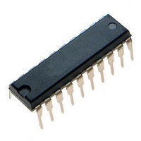
MCHC705JJ7CPE Freescale Semiconductor, MCHC705JJ7CPE Datasheet - Page 83

MCHC705JJ7CPE
Manufacturer Part Number
MCHC705JJ7CPE
Description
IC MCU 8BIT 224 BYTES RAM 20PDIP
Manufacturer
Freescale Semiconductor
Series
HC05r
Datasheet
1.MC705JJ7CDWE.pdf
(164 pages)
Specifications of MCHC705JJ7CPE
Core Processor
HC05
Core Size
8-Bit
Speed
2.1MHz
Connectivity
SIO
Peripherals
POR, Temp Sensor, WDT
Number Of I /o
14
Program Memory Size
6KB (6K x 8)
Program Memory Type
OTP
Ram Size
224 x 8
Voltage - Supply (vcc/vdd)
2.7 V ~ 5.5 V
Data Converters
A/D 4x12b
Oscillator Type
Internal
Operating Temperature
-40°C ~ 85°C
Package / Case
20-DIP (0.300", 7.62mm)
Processor Series
HC705JJ
Core
HC05
Data Bus Width
8 bit
Data Ram Size
224 B
Interface Type
SIOP
Maximum Clock Frequency
2.1 MHz
Number Of Programmable I/os
14
Number Of Timers
2
Maximum Operating Temperature
+ 85 C
Mounting Style
Through Hole
Minimum Operating Temperature
- 40 C
On-chip Adc
12 bit, 4 Channel
Package
20PDIP
Family Name
HC05
Maximum Speed
2.1 MHz
Operating Supply Voltage
3.3|5 V
Lead Free Status / RoHS Status
Lead free / RoHS Compliant
Eeprom Size
-
Lead Free Status / Rohs Status
Details
The full scale voltage range for a given capacitance, f
as:
Once charged to a given voltage, a finite amount of time will be required to discharge the capacitor back
to its start voltage at V
the sinking current of the internal discharge device. To allow a reasonable time for the capacitor to return
to V
attached to the PB0 pin. If the total charge/discharge cycle time is critical, then the discharge time should
be at least 1/10 of the most recent charge time. Shorter discharge times may be used if lesser accuracy
in the voltage measurement is acceptable.
Table 8-4
some A/D conversion examples for several bit resolutions.
The mode selection bits in the ACR allow four methods of single-slope A/D conversion. Each of these
methods is shown in
Table
Freescale Semiconductor
Name
V
C
I
t
I
t
CHG
CHG
V
MAX
•
•
•
•
DIS
DIS
EXT
N
SS
X
8-4.
Manual start and stop (mode 0)
Manual start and automatic discharge (mode 1)
Automatic start and stop from TOF to ICF (mode 2)
Automatic start and stop from OCF to ICF (mode 3)
levels, the discharge time should last about 10 milliseconds per microfarad of capacitance
Unknown voltage on channel selection bus
Maximum charging voltage on external capacitor
Charging current on external ramping capacitor
Discharge current on external ramping capacitor
Time to charge external capacitor
(100 kHz < f
Time to discharge external capacitor, C
Capacitance of external ramping capacitor
Number of counts for I
gives the range of values of each parameter in the A/D timing conversion and
V
V
4-bit result
6-bit result
8-bit result
10-bit result
12-bit result
DD
DD
Sufficient time should be allowed to discharge the external capacitor or
subsequent charge times will be shortened with resultant errors in timing
conversion.
= 3 Vdc
= 5 Vdc
OSC
MC68HC705JJ7 • MC68HC705JP7 Advance Information Data Sheet, Rev. 4.1
Figure 8-8
SS
< 4.0 MHz)
. This discharge time will be solely based on the value of capacitance used and
Function
CHG
to charge C
Table 8-4. A/D Conversion Parameters
V
through
FS
= N
Figure 8-8
EXT
Figure 8-11
FS
EXT
to V
x P x I
X
NOTE
CHG
Refer to
Refer to
using the signal names and parameters given in
OSC
Figure 8-9
0.0001
0.032
0.128
0.512
2.048
8.192
/ (C
Min
V
15.10 Analog Subsystem Characteristics (3.0 Vdc)
15.10 Analog Subsystem Characteristics (3.0 Vdc)
—
—
, conversion method, and resolution is defined
1
SS
Figure 8-10
15.9 Analog Subsystem Characteristics (5.0 Vdc)
15.9 Analog Subsystem Characteristics (5.0 Vdc)
Figure 8-11
EXT
x f
OSC
32.768
0.128
0.512
2.048
8.196
1024
Typ
)
0.1
—
—
5
A/D Conversion Methods
Continued on next page
V
V
65536
DD
DD
120
120
10.24
40.96
Max
2.56
2.0
10
–1.5
–1.5
Table 8-5
(1)
(1)
Counts
ms/µF
Units
gives
ms
µF
V
V
and
and
83


