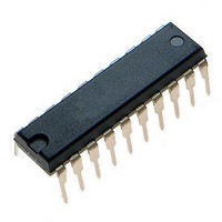
MCHC705JJ7CPE Freescale Semiconductor, MCHC705JJ7CPE Datasheet - Page 77

MCHC705JJ7CPE
Manufacturer Part Number
MCHC705JJ7CPE
Description
IC MCU 8BIT 224 BYTES RAM 20PDIP
Manufacturer
Freescale Semiconductor
Series
HC05r
Datasheet
1.MC705JJ7CDWE.pdf
(164 pages)
Specifications of MCHC705JJ7CPE
Core Processor
HC05
Core Size
8-Bit
Speed
2.1MHz
Connectivity
SIO
Peripherals
POR, Temp Sensor, WDT
Number Of I /o
14
Program Memory Size
6KB (6K x 8)
Program Memory Type
OTP
Ram Size
224 x 8
Voltage - Supply (vcc/vdd)
2.7 V ~ 5.5 V
Data Converters
A/D 4x12b
Oscillator Type
Internal
Operating Temperature
-40°C ~ 85°C
Package / Case
20-DIP (0.300", 7.62mm)
Processor Series
HC705JJ
Core
HC05
Data Bus Width
8 bit
Data Ram Size
224 B
Interface Type
SIOP
Maximum Clock Frequency
2.1 MHz
Number Of Programmable I/os
14
Number Of Timers
2
Maximum Operating Temperature
+ 85 C
Mounting Style
Through Hole
Minimum Operating Temperature
- 40 C
On-chip Adc
12 bit, 4 Channel
Package
20PDIP
Family Name
HC05
Maximum Speed
2.1 MHz
Operating Supply Voltage
3.3|5 V
Lead Free Status / RoHS Status
Lead free / RoHS Compliant
Eeprom Size
-
Lead Free Status / Rohs Status
Details
- Current page: 77 of 164
- Download datasheet (2Mb)
CHG
ATD1–ATD2
Freescale Semiconductor
The CHG enable bit allows direct control of the charge current source and the discharge device and
also reflects the state of the discharge device. This bit is cleared by a reset of the device.
The ATD1–ATD2 enable bits select one of the four operating modes used for making A/D conversions
via the single-slope method.These four modes are given in
ISEN enable bit is cleared. These bits are cleared by a reset of the device and thereby return the
analog subsystem to the manual A/D conversion method.
1 = If the ISEN bit is also set, the charge current source is sourcing current out of the PB0/AN0 pin.
0 = The discharge device is sinking current into the PB0/AN0 pin. Writing a logic 0 disables the
Writing a logic 1 enables the charging current out of the PB0/AN0 pin.
charging current and enables the discharging current into the PB0/AN0 pin, if the ISEN bit is
also set.
Address:
Disabled
Option
Reset:
Mode
Read:
Write:
A/D
3
MC68HC705JJ7 • MC68HC705JP7 Advance Information Data Sheet, Rev. 4.1
$001D
CHG
Bit 7
synchronized
0
source and
charge and
(OCF–ICF)
Automatic
discharge
discharge
disabled
Control
Charge
Current
to timer
Figure 8-5. Analog Control Register (ACR)
ATD2
Table 8-3. A/D Conversion Options
6
0
ISEN
0
1
1
1
1
ATD1
5
0
ATD2
A/D Options
X
0
1
1
1
ICEN
4
0
ATD1
X
0
0
1
1
CPIE
3
0
CHG
Table
X
1
1
0
1
CP2EN
Current control disabled,
no source or sink current
Begin sourcing current
when the CHG bit is set
and continue to source
current until the CHG bit is
cleared.
The CHG bit remains set
until the next time ICF
occurs.
The CHG bit remains
cleared until the next time
OCF occurs.
The CHG bit remains set
until the next time ICF
occurs.
8-3. These bits have no effect if the
2
0
to/from PB0/AN0
Current Flow
CP1EN
1
0
Analog Control Register
ISEN
Bit 0
0
77
Related parts for MCHC705JJ7CPE
Image
Part Number
Description
Manufacturer
Datasheet
Request
R
Part Number:
Description:
Manufacturer:
Freescale Semiconductor, Inc
Datasheet:
Part Number:
Description:
Manufacturer:
Freescale Semiconductor, Inc
Datasheet:
Part Number:
Description:
Manufacturer:
Freescale Semiconductor, Inc
Datasheet:
Part Number:
Description:
Manufacturer:
Freescale Semiconductor, Inc
Datasheet:
Part Number:
Description:
Manufacturer:
Freescale Semiconductor, Inc
Datasheet:
Part Number:
Description:
Manufacturer:
Freescale Semiconductor, Inc
Datasheet:
Part Number:
Description:
Manufacturer:
Freescale Semiconductor, Inc
Datasheet:
Part Number:
Description:
Manufacturer:
Freescale Semiconductor, Inc
Datasheet:
Part Number:
Description:
Manufacturer:
Freescale Semiconductor, Inc
Datasheet:
Part Number:
Description:
Manufacturer:
Freescale Semiconductor, Inc
Datasheet:
Part Number:
Description:
Manufacturer:
Freescale Semiconductor, Inc
Datasheet:
Part Number:
Description:
Manufacturer:
Freescale Semiconductor, Inc
Datasheet:
Part Number:
Description:
Manufacturer:
Freescale Semiconductor, Inc
Datasheet:
Part Number:
Description:
Manufacturer:
Freescale Semiconductor, Inc
Datasheet:
Part Number:
Description:
Manufacturer:
Freescale Semiconductor, Inc
Datasheet:


