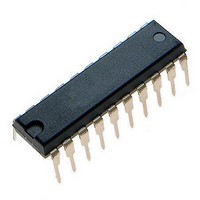
MCHC705JJ7CPE Freescale Semiconductor, MCHC705JJ7CPE Datasheet - Page 64

MCHC705JJ7CPE
Manufacturer Part Number
MCHC705JJ7CPE
Description
IC MCU 8BIT 224 BYTES RAM 20PDIP
Manufacturer
Freescale Semiconductor
Series
HC05r
Datasheet
1.MC705JJ7CDWE.pdf
(164 pages)
Specifications of MCHC705JJ7CPE
Core Processor
HC05
Core Size
8-Bit
Speed
2.1MHz
Connectivity
SIO
Peripherals
POR, Temp Sensor, WDT
Number Of I /o
14
Program Memory Size
6KB (6K x 8)
Program Memory Type
OTP
Ram Size
224 x 8
Voltage - Supply (vcc/vdd)
2.7 V ~ 5.5 V
Data Converters
A/D 4x12b
Oscillator Type
Internal
Operating Temperature
-40°C ~ 85°C
Package / Case
20-DIP (0.300", 7.62mm)
Processor Series
HC705JJ
Core
HC05
Data Bus Width
8 bit
Data Ram Size
224 B
Interface Type
SIOP
Maximum Clock Frequency
2.1 MHz
Number Of Programmable I/os
14
Number Of Timers
2
Maximum Operating Temperature
+ 85 C
Mounting Style
Through Hole
Minimum Operating Temperature
- 40 C
On-chip Adc
12 bit, 4 Channel
Package
20PDIP
Family Name
HC05
Maximum Speed
2.1 MHz
Operating Supply Voltage
3.3|5 V
Lead Free Status / RoHS Status
Lead free / RoHS Compliant
Eeprom Size
-
Lead Free Status / Rohs Status
Details
- Current page: 64 of 164
- Download datasheet (2Mb)
Parallel Input/Output
7.3.8 PB6/SDI Logic
The PB6/SDI pin can be used as a simple I/O port pin or be controlled by the SIOP serial interface as
shown in
When using the PB6/SDI pin, these interactions must be noted:
64
1. If the SIOP function is required, then the SPE bit in the SCR must be set. This causes the PB6/SDI
2. If the SIOP function is in control of the PB6/SDI pin, the DDRB6 and PB6 data register bits are still
3. If the SIOP function is terminated by clearing the SPE bit in the SCR, then the last conditions stored
4. If the PB6/SDI pin is to be a digital input, then both the SPE bit in the SCR and the DDRB6 bit must
5. If the PB6/SDI pin is to be a digital output, then the SPE bit in the SCR must be cleared and the
pin buffer to be disabled to allow the PB6/SDI pin to act as an input that feeds the serial data input
(SDI) of the SIOP. The pulldown device is disabled in this case.
accessible to the CPU and can be altered or read without affecting the SIOP functionality.
However, if the DDRB6 bit is cleared, reading the PB6 data register will return the current state of
the PB6/SDI pin.
in the DDRB6, PDIB6, and PB6 register bits will then control the PB6/SDI pin.
be cleared. Depending on the external application, the pulldown device may also be disabled by
setting the PDIB6 pulldown inhibit bit.
DDRB6 bit must be set. The pulldown device will be disabled in this case.
Figure
WRITE $0005
WRITE $0001
WRITE $0011
RESET
READ $0005
READ $0001
7-11. The operations of PB6/SDI pin are summarized in
MC68HC705JJ7 • MC68HC705JP7 Advance Information Data Sheet, Rev. 4.1
SERIAL DATA IN (SDI)
SERIAL ENABLE (SPE)
R
R
PORT B DATA
Figure 7-11. PB6/SDI Pin I/O Circuit
REGISTER
DATA DIRECTION
BIT PB6
REGISTER B
REGISTER B
PULLDOWN
BIT DDRB6
BIT PDIB6
MASK OPTION REG. ($1FF1)
Table
7-3.
Freescale Semiconductor
PULLDOWN
DEVICE
PB6
SDI
Related parts for MCHC705JJ7CPE
Image
Part Number
Description
Manufacturer
Datasheet
Request
R
Part Number:
Description:
Manufacturer:
Freescale Semiconductor, Inc
Datasheet:
Part Number:
Description:
Manufacturer:
Freescale Semiconductor, Inc
Datasheet:
Part Number:
Description:
Manufacturer:
Freescale Semiconductor, Inc
Datasheet:
Part Number:
Description:
Manufacturer:
Freescale Semiconductor, Inc
Datasheet:
Part Number:
Description:
Manufacturer:
Freescale Semiconductor, Inc
Datasheet:
Part Number:
Description:
Manufacturer:
Freescale Semiconductor, Inc
Datasheet:
Part Number:
Description:
Manufacturer:
Freescale Semiconductor, Inc
Datasheet:
Part Number:
Description:
Manufacturer:
Freescale Semiconductor, Inc
Datasheet:
Part Number:
Description:
Manufacturer:
Freescale Semiconductor, Inc
Datasheet:
Part Number:
Description:
Manufacturer:
Freescale Semiconductor, Inc
Datasheet:
Part Number:
Description:
Manufacturer:
Freescale Semiconductor, Inc
Datasheet:
Part Number:
Description:
Manufacturer:
Freescale Semiconductor, Inc
Datasheet:
Part Number:
Description:
Manufacturer:
Freescale Semiconductor, Inc
Datasheet:
Part Number:
Description:
Manufacturer:
Freescale Semiconductor, Inc
Datasheet:
Part Number:
Description:
Manufacturer:
Freescale Semiconductor, Inc
Datasheet:


