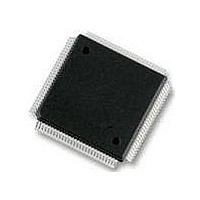
MC9S12DT256MPVE Freescale Semiconductor, MC9S12DT256MPVE Datasheet - Page 189

MC9S12DT256MPVE
Manufacturer Part Number
MC9S12DT256MPVE
Description
IC MCU 256K FLASH 25MHZ 112-LQFP
Manufacturer
Freescale Semiconductor
Series
HCS12r
Datasheet
1.S912XDG128F2MAL.pdf
(1348 pages)
Specifications of MC9S12DT256MPVE
Core Processor
HCS12
Core Size
16-Bit
Speed
25MHz
Connectivity
CAN, I²C, SCI, SPI
Peripherals
PWM, WDT
Number Of I /o
91
Program Memory Size
256KB (256K x 8)
Program Memory Type
FLASH
Eeprom Size
4K x 8
Ram Size
12K x 8
Voltage - Supply (vcc/vdd)
2.35 V ~ 5.25 V
Data Converters
A/D 8x10b
Oscillator Type
Internal
Operating Temperature
-40°C ~ 125°C
Package / Case
112-LQFP
Processor Series
S12D
Core
HCS12
Data Bus Width
16 bit
Data Ram Size
12 KB
Interface Type
CAN/I2C/SCI/SPI
Maximum Clock Frequency
25 MHz
Number Of Programmable I/os
91
Number Of Timers
1
Operating Supply Voltage
5 V to 2.5 V
Maximum Operating Temperature
+ 125 C
Mounting Style
SMD/SMT
3rd Party Development Tools
EWHCS12
Development Tools By Supplier
M68KIT912DP256
Minimum Operating Temperature
- 40 C
On-chip Adc
2 (8-ch x 10-bit)
No. Of I/o's
91
Eeprom Memory Size
4KB
Ram Memory Size
12KB
Cpu Speed
25MHz
No. Of Timers
1
No. Of Pwm Channels
8
Digital Ic Case Style
LQFP
Rohs Compliant
Yes
Lead Free Status / RoHS Status
Lead free / RoHS Compliant
Available stocks
Company
Part Number
Manufacturer
Quantity
Price
Company:
Part Number:
MC9S12DT256MPVE
Manufacturer:
Freescale Semiconductor
Quantity:
10 000
- Current page: 189 of 1348
- Download datasheet (8Mb)
6.3.1.1
All module level switches and flags are located in the module control register
Read: Anytime
Write: Anytime
Freescale Semiconductor
Reset
XGDBGM
XGFRZM
XGSSM
XGEM
Field
W
R
15
14
13
12
XGEM
15
0
0
XGE Mask — This bit controls the write access to the XGE bit. The XGE bit can only be set or cleared if a "1" is
written to the XGEM bit in the same register access.
Read:
Write:
0 Disable write access to the XGE in the same bus cycle
1 Enable write access to the XGE in the same bus cycle
XGFRZ Mask — This bit controls the write access to the XGFRZ bit. The XGFRZ bit can only be set or cleared
if a "1" is written to the XGFRZM bit in the same register access.
Read:
Write:
0 Disable write access to the XGFRZ in the same bus cycle
1 Enable write access to the XGFRZ in the same bus cycle
XGDBG Mask — This bit controls the write access to the XGDBG bit. The XGDBG bit can only be set or cleared
if a "1" is written to the XGDBGM bit in the same register access.
Read:
Write:
0 Disable write access to the XGDBG in the same bus cycle
1 Enable write access to the XGDBG in the same bus cycle
XGSS Mask — This bit controls the write access to the XGSS bit. The XGSS bit can only be set or cleared if a
"1" is written to the XGSSM bit in the same register access.
Read:
Write:
0 Disable write access to the XGSS in the same bus cycle
1 Enable write access to the XGSS in the same bus cycle
FRZM
XGATE Control Register (XGMCTL)
XG
14
0
0
This bit will always read "0".
This bit will always read "0".
This bit will always read "0".
This bit will always read "0".
= Unimplemented or Reserved
DBGM
XG
13
0
0
SSM
XG
12
Table 6-1. XGMCTL Field Descriptions (Sheet 1 of 3)
0
0
Figure 6-3. XGATE Control Register (XGMCTL)
FACTM
XG
11
0
0
MC9S12XDP512 Data Sheet, Rev. 2.21
10
0
0
SWEIFM
XG
0
0
9
XGIEM
0
0
8
Description
XGE XGFRZ XGDBG XGSS XGFACT
7
0
0
6
0
5
0
4
Figure
Chapter 6 XGATE (S12XGATEV2)
0
3
6-3.
2
0
0
SWEIF
XG
0
1
XGIE
0
0
189
Related parts for MC9S12DT256MPVE
Image
Part Number
Description
Manufacturer
Datasheet
Request
R
Part Number:
Description:
Manufacturer:
Freescale Semiconductor, Inc
Datasheet:
Part Number:
Description:
Manufacturer:
Freescale Semiconductor, Inc
Datasheet:
Part Number:
Description:
Manufacturer:
Freescale Semiconductor, Inc
Datasheet:
Part Number:
Description:
Manufacturer:
Freescale Semiconductor, Inc
Datasheet:
Part Number:
Description:
Manufacturer:
Freescale Semiconductor, Inc
Datasheet:
Part Number:
Description:
Manufacturer:
Freescale Semiconductor, Inc
Datasheet:
Part Number:
Description:
Manufacturer:
Freescale Semiconductor, Inc
Datasheet:
Part Number:
Description:
Manufacturer:
Freescale Semiconductor, Inc
Datasheet:
Part Number:
Description:
Manufacturer:
Freescale Semiconductor, Inc
Datasheet:
Part Number:
Description:
Manufacturer:
Freescale Semiconductor, Inc
Datasheet:
Part Number:
Description:
Manufacturer:
Freescale Semiconductor, Inc
Datasheet:
Part Number:
Description:
Manufacturer:
Freescale Semiconductor, Inc
Datasheet:
Part Number:
Description:
Manufacturer:
Freescale Semiconductor, Inc
Datasheet:
Part Number:
Description:
Manufacturer:
Freescale Semiconductor, Inc
Datasheet:
Part Number:
Description:
Manufacturer:
Freescale Semiconductor, Inc
Datasheet:


