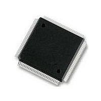
MC9S12DT256MPVE Freescale Semiconductor, MC9S12DT256MPVE Datasheet - Page 900

MC9S12DT256MPVE
Manufacturer Part Number
MC9S12DT256MPVE
Description
IC MCU 256K FLASH 25MHZ 112-LQFP
Manufacturer
Freescale Semiconductor
Series
HCS12r
Datasheet
1.S912XDG128F2MAL.pdf
(1348 pages)
Specifications of MC9S12DT256MPVE
Core Processor
HCS12
Core Size
16-Bit
Speed
25MHz
Connectivity
CAN, I²C, SCI, SPI
Peripherals
PWM, WDT
Number Of I /o
91
Program Memory Size
256KB (256K x 8)
Program Memory Type
FLASH
Eeprom Size
4K x 8
Ram Size
12K x 8
Voltage - Supply (vcc/vdd)
2.35 V ~ 5.25 V
Data Converters
A/D 8x10b
Oscillator Type
Internal
Operating Temperature
-40°C ~ 125°C
Package / Case
112-LQFP
Processor Series
S12D
Core
HCS12
Data Bus Width
16 bit
Data Ram Size
12 KB
Interface Type
CAN/I2C/SCI/SPI
Maximum Clock Frequency
25 MHz
Number Of Programmable I/os
91
Number Of Timers
1
Operating Supply Voltage
5 V to 2.5 V
Maximum Operating Temperature
+ 125 C
Mounting Style
SMD/SMT
3rd Party Development Tools
EWHCS12
Development Tools By Supplier
M68KIT912DP256
Minimum Operating Temperature
- 40 C
On-chip Adc
2 (8-ch x 10-bit)
No. Of I/o's
91
Eeprom Memory Size
4KB
Ram Memory Size
12KB
Cpu Speed
25MHz
No. Of Timers
1
No. Of Pwm Channels
8
Digital Ic Case Style
LQFP
Rohs Compliant
Yes
Lead Free Status / RoHS Status
Lead free / RoHS Compliant
Available stocks
Company
Part Number
Manufacturer
Quantity
Price
Company:
Part Number:
MC9S12DT256MPVE
Manufacturer:
Freescale Semiconductor
Quantity:
10 000
- Current page: 900 of 1348
- Download datasheet (8Mb)
Chapter 23 DQ256 Port Integration Module (S12XDQ256PIMV2)
A standard port pin has the following minimum features:
Optional features:
23.0.2
Figure 23-1
902
•
•
•
•
•
•
•
•
•
•
•
•
•
•
•
•
•
•
•
•
Control registers to enable/disable pull-device and select pull-ups/pull-downs on Ports T, S, M, P,
H, and J on per-pin basis
Control registers to enable/disable pull-up devices on Ports AD0, and AD1 on per-pin basis
Single control register to enable/disable pull-ups on Ports A, B, C, D, E, and K on per-port basis
and on BKGD pin
Control registers to enable/disable reduced output drive on Ports T, S, M, P, H, J, AD0, and AD1
on per-pin basis
Single control register to enable/disable reduced output drive on Ports A, B, C, D, E, and K on per-
port basis
Control registers to enable/disable open-drain (wired-OR) mode on Ports S and M
Control registers to enable/disable pin interrupts on Ports P, H, and J
Interrupt flag register for pin interrupts on Ports P, H, and J
Control register to configure IRQ pin operation
Free-running clock outputs
Input/output selection
5V output drive with two selectable drive strengths
5V digital and analog input
Input with selectable pull-up or pull-down device
Open drain for wired-OR connections
Interrupt inputs with glitch filtering
Reduced input threshold to support low voltage applications
Signals shown in Bold are not available in 80-pin packages.
Signals shown in Bold-Italics are neither available in 112-pin nor in 80-pin packages.
Shaded labels denote alternative module routing ports.
Block Diagram
is a block diagram of the PIM.
MC9S12XDP512 Data Sheet, Rev. 2.21
Freescale Semiconductor
Related parts for MC9S12DT256MPVE
Image
Part Number
Description
Manufacturer
Datasheet
Request
R
Part Number:
Description:
Manufacturer:
Freescale Semiconductor, Inc
Datasheet:
Part Number:
Description:
Manufacturer:
Freescale Semiconductor, Inc
Datasheet:
Part Number:
Description:
Manufacturer:
Freescale Semiconductor, Inc
Datasheet:
Part Number:
Description:
Manufacturer:
Freescale Semiconductor, Inc
Datasheet:
Part Number:
Description:
Manufacturer:
Freescale Semiconductor, Inc
Datasheet:
Part Number:
Description:
Manufacturer:
Freescale Semiconductor, Inc
Datasheet:
Part Number:
Description:
Manufacturer:
Freescale Semiconductor, Inc
Datasheet:
Part Number:
Description:
Manufacturer:
Freescale Semiconductor, Inc
Datasheet:
Part Number:
Description:
Manufacturer:
Freescale Semiconductor, Inc
Datasheet:
Part Number:
Description:
Manufacturer:
Freescale Semiconductor, Inc
Datasheet:
Part Number:
Description:
Manufacturer:
Freescale Semiconductor, Inc
Datasheet:
Part Number:
Description:
Manufacturer:
Freescale Semiconductor, Inc
Datasheet:
Part Number:
Description:
Manufacturer:
Freescale Semiconductor, Inc
Datasheet:
Part Number:
Description:
Manufacturer:
Freescale Semiconductor, Inc
Datasheet:
Part Number:
Description:
Manufacturer:
Freescale Semiconductor, Inc
Datasheet:


