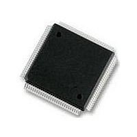
MC9S12DT256MPVE Freescale Semiconductor, MC9S12DT256MPVE Datasheet - Page 97

MC9S12DT256MPVE
Manufacturer Part Number
MC9S12DT256MPVE
Description
IC MCU 256K FLASH 25MHZ 112-LQFP
Manufacturer
Freescale Semiconductor
Series
HCS12r
Datasheet
1.S912XDG128F2MAL.pdf
(1348 pages)
Specifications of MC9S12DT256MPVE
Core Processor
HCS12
Core Size
16-Bit
Speed
25MHz
Connectivity
CAN, I²C, SCI, SPI
Peripherals
PWM, WDT
Number Of I /o
91
Program Memory Size
256KB (256K x 8)
Program Memory Type
FLASH
Eeprom Size
4K x 8
Ram Size
12K x 8
Voltage - Supply (vcc/vdd)
2.35 V ~ 5.25 V
Data Converters
A/D 8x10b
Oscillator Type
Internal
Operating Temperature
-40°C ~ 125°C
Package / Case
112-LQFP
Processor Series
S12D
Core
HCS12
Data Bus Width
16 bit
Data Ram Size
12 KB
Interface Type
CAN/I2C/SCI/SPI
Maximum Clock Frequency
25 MHz
Number Of Programmable I/os
91
Number Of Timers
1
Operating Supply Voltage
5 V to 2.5 V
Maximum Operating Temperature
+ 125 C
Mounting Style
SMD/SMT
3rd Party Development Tools
EWHCS12
Development Tools By Supplier
M68KIT912DP256
Minimum Operating Temperature
- 40 C
On-chip Adc
2 (8-ch x 10-bit)
No. Of I/o's
91
Eeprom Memory Size
4KB
Ram Memory Size
12KB
Cpu Speed
25MHz
No. Of Timers
1
No. Of Pwm Channels
8
Digital Ic Case Style
LQFP
Rohs Compliant
Yes
Lead Free Status / RoHS Status
Lead free / RoHS Compliant
Available stocks
Company
Part Number
Manufacturer
Quantity
Price
Company:
Part Number:
MC9S12DT256MPVE
Manufacturer:
Freescale Semiconductor
Quantity:
10 000
- Current page: 97 of 1348
- Download datasheet (8Mb)
2.3.2.12
This register is used to restart the COP time-out period.
Read: Always reads 0x_00
Write: Anytime
When the COP is disabled (CR[2:0] = “000”) writing to this register has no effect.
When the COP is enabled by setting CR[2:0] nonzero, the following applies:
Freescale Semiconductor
Reset
W
R
Writing any value other than 0x_55 or 0x_AA causes a COP reset. To restart the COP time-out
period you must write 0x_55 followed by a write of 0x_AA. Other instructions may be executed
between these writes but the sequence (0x_55, 0x_AA) must be completed prior to COP end of
time-out period to avoid a COP reset. Sequences of 0x_55 writes or sequences of 0x_AA writes
are allowed. When the WCOP bit is set, 0x_55 and 0x_AA writes must be done in the last 25% of
the selected time-out period; writing any value in the first 75% of the selected period will cause a
COP reset.
Bit 7
CRG COP Timer Arm/Reset Register (ARMCOP)
0
0
7
Bit 6
0
0
6
Figure 2-15. ARMCOP Register Diagram
MC9S12XDP512 Data Sheet, Rev. 2.21
Bit 5
0
0
5
Bit 4
0
0
4
Bit 3
0
0
3
Chapter 2 Clocks and Reset Generator (S12CRGV6)
Bit 2
0
0
2
Bit 1
0
0
1
Bit 0
0
0
0
97
Related parts for MC9S12DT256MPVE
Image
Part Number
Description
Manufacturer
Datasheet
Request
R
Part Number:
Description:
Manufacturer:
Freescale Semiconductor, Inc
Datasheet:
Part Number:
Description:
Manufacturer:
Freescale Semiconductor, Inc
Datasheet:
Part Number:
Description:
Manufacturer:
Freescale Semiconductor, Inc
Datasheet:
Part Number:
Description:
Manufacturer:
Freescale Semiconductor, Inc
Datasheet:
Part Number:
Description:
Manufacturer:
Freescale Semiconductor, Inc
Datasheet:
Part Number:
Description:
Manufacturer:
Freescale Semiconductor, Inc
Datasheet:
Part Number:
Description:
Manufacturer:
Freescale Semiconductor, Inc
Datasheet:
Part Number:
Description:
Manufacturer:
Freescale Semiconductor, Inc
Datasheet:
Part Number:
Description:
Manufacturer:
Freescale Semiconductor, Inc
Datasheet:
Part Number:
Description:
Manufacturer:
Freescale Semiconductor, Inc
Datasheet:
Part Number:
Description:
Manufacturer:
Freescale Semiconductor, Inc
Datasheet:
Part Number:
Description:
Manufacturer:
Freescale Semiconductor, Inc
Datasheet:
Part Number:
Description:
Manufacturer:
Freescale Semiconductor, Inc
Datasheet:
Part Number:
Description:
Manufacturer:
Freescale Semiconductor, Inc
Datasheet:
Part Number:
Description:
Manufacturer:
Freescale Semiconductor, Inc
Datasheet:


