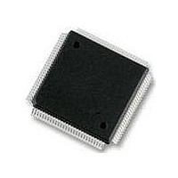
MC9S12DT256MPVE Freescale Semiconductor, MC9S12DT256MPVE Datasheet - Page 564

MC9S12DT256MPVE
Manufacturer Part Number
MC9S12DT256MPVE
Description
IC MCU 256K FLASH 25MHZ 112-LQFP
Manufacturer
Freescale Semiconductor
Series
HCS12r
Datasheet
1.S912XDG128F2MAL.pdf
(1348 pages)
Specifications of MC9S12DT256MPVE
Core Processor
HCS12
Core Size
16-Bit
Speed
25MHz
Connectivity
CAN, I²C, SCI, SPI
Peripherals
PWM, WDT
Number Of I /o
91
Program Memory Size
256KB (256K x 8)
Program Memory Type
FLASH
Eeprom Size
4K x 8
Ram Size
12K x 8
Voltage - Supply (vcc/vdd)
2.35 V ~ 5.25 V
Data Converters
A/D 8x10b
Oscillator Type
Internal
Operating Temperature
-40°C ~ 125°C
Package / Case
112-LQFP
Processor Series
S12D
Core
HCS12
Data Bus Width
16 bit
Data Ram Size
12 KB
Interface Type
CAN/I2C/SCI/SPI
Maximum Clock Frequency
25 MHz
Number Of Programmable I/os
91
Number Of Timers
1
Operating Supply Voltage
5 V to 2.5 V
Maximum Operating Temperature
+ 125 C
Mounting Style
SMD/SMT
3rd Party Development Tools
EWHCS12
Development Tools By Supplier
M68KIT912DP256
Minimum Operating Temperature
- 40 C
On-chip Adc
2 (8-ch x 10-bit)
No. Of I/o's
91
Eeprom Memory Size
4KB
Ram Memory Size
12KB
Cpu Speed
25MHz
No. Of Timers
1
No. Of Pwm Channels
8
Digital Ic Case Style
LQFP
Rohs Compliant
Yes
Lead Free Status / RoHS Status
Lead free / RoHS Compliant
Available stocks
Company
Part Number
Manufacturer
Quantity
Price
Company:
Part Number:
MC9S12DT256MPVE
Manufacturer:
Freescale Semiconductor
Quantity:
10 000
- Current page: 564 of 1348
- Download datasheet (8Mb)
Chapter 14 Voltage Regulator (S12VREG3V3V5)
14.3.2.6
The Reserved 06 is reserved for test purposes.
14.3.2.7
The Reserved 07 is reserved for test purposes.
14.4
14.4.1
Module VREG_3V3 is a voltage regulator, as depicted in
are the regulator core (REG), a low-voltage detect module (LVD), a control block (CTRL), a power-on
reset module (POR), and a low-voltage reset module (LVR).
14.4.2
Respectively its regulator core has two parallel, independent regulation loops (REG1 and REG2) that differ
only in the amount of current that can be delivered.
The regulator is a linear regulator with a bandgap reference when operated in Full Performance Mode. It
acts as a voltage clamp in Reduced Power Mode. All load currents flow from input V
V
14.4.2.1
In Full Performance Mode, the output voltage is compared with a reference voltage by an operational
amplifier. The amplified input voltage difference drives the gate of an output transistor.
564
SSPLL
Reset
Reset
W
W
R
R
. The reference circuits are supplied by V
Functional Description
General
Regulator Core (REG)
Reserved 06
Reserved 07
Full Performance Mode
0
0
0
0
7
7
= Unimplemented or Reserved
= Unimplemented or Reserved
0
0
0
0
6
6
MC9S12XDP512 Data Sheet, Rev. 2.21
0
0
0
0
5
5
Figure 14-8. Reserved 06
Figure 14-9. Reserved 07
DDA
0
0
0
0
4
4
and V
Figure
SSA
0
0
0
0
3
3
.
14-1. The regulator functional elements
0
0
0
0
2
2
Freescale Semiconductor
DDR
0
0
0
0
1
1
to V
SS
or
0
0
0
0
0
0
Related parts for MC9S12DT256MPVE
Image
Part Number
Description
Manufacturer
Datasheet
Request
R
Part Number:
Description:
Manufacturer:
Freescale Semiconductor, Inc
Datasheet:
Part Number:
Description:
Manufacturer:
Freescale Semiconductor, Inc
Datasheet:
Part Number:
Description:
Manufacturer:
Freescale Semiconductor, Inc
Datasheet:
Part Number:
Description:
Manufacturer:
Freescale Semiconductor, Inc
Datasheet:
Part Number:
Description:
Manufacturer:
Freescale Semiconductor, Inc
Datasheet:
Part Number:
Description:
Manufacturer:
Freescale Semiconductor, Inc
Datasheet:
Part Number:
Description:
Manufacturer:
Freescale Semiconductor, Inc
Datasheet:
Part Number:
Description:
Manufacturer:
Freescale Semiconductor, Inc
Datasheet:
Part Number:
Description:
Manufacturer:
Freescale Semiconductor, Inc
Datasheet:
Part Number:
Description:
Manufacturer:
Freescale Semiconductor, Inc
Datasheet:
Part Number:
Description:
Manufacturer:
Freescale Semiconductor, Inc
Datasheet:
Part Number:
Description:
Manufacturer:
Freescale Semiconductor, Inc
Datasheet:
Part Number:
Description:
Manufacturer:
Freescale Semiconductor, Inc
Datasheet:
Part Number:
Description:
Manufacturer:
Freescale Semiconductor, Inc
Datasheet:
Part Number:
Description:
Manufacturer:
Freescale Semiconductor, Inc
Datasheet:


