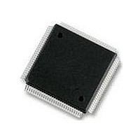
MC9S12DT256MPVE Freescale Semiconductor, MC9S12DT256MPVE Datasheet - Page 381

MC9S12DT256MPVE
Manufacturer Part Number
MC9S12DT256MPVE
Description
IC MCU 256K FLASH 25MHZ 112-LQFP
Manufacturer
Freescale Semiconductor
Series
HCS12r
Datasheet
1.S912XDG128F2MAL.pdf
(1348 pages)
Specifications of MC9S12DT256MPVE
Core Processor
HCS12
Core Size
16-Bit
Speed
25MHz
Connectivity
CAN, I²C, SCI, SPI
Peripherals
PWM, WDT
Number Of I /o
91
Program Memory Size
256KB (256K x 8)
Program Memory Type
FLASH
Eeprom Size
4K x 8
Ram Size
12K x 8
Voltage - Supply (vcc/vdd)
2.35 V ~ 5.25 V
Data Converters
A/D 8x10b
Oscillator Type
Internal
Operating Temperature
-40°C ~ 125°C
Package / Case
112-LQFP
Processor Series
S12D
Core
HCS12
Data Bus Width
16 bit
Data Ram Size
12 KB
Interface Type
CAN/I2C/SCI/SPI
Maximum Clock Frequency
25 MHz
Number Of Programmable I/os
91
Number Of Timers
1
Operating Supply Voltage
5 V to 2.5 V
Maximum Operating Temperature
+ 125 C
Mounting Style
SMD/SMT
3rd Party Development Tools
EWHCS12
Development Tools By Supplier
M68KIT912DP256
Minimum Operating Temperature
- 40 C
On-chip Adc
2 (8-ch x 10-bit)
No. Of I/o's
91
Eeprom Memory Size
4KB
Ram Memory Size
12KB
Cpu Speed
25MHz
No. Of Timers
1
No. Of Pwm Channels
8
Digital Ic Case Style
LQFP
Rohs Compliant
Yes
Lead Free Status / RoHS Status
Lead free / RoHS Compliant
Available stocks
Company
Part Number
Manufacturer
Quantity
Price
Company:
Part Number:
MC9S12DT256MPVE
Manufacturer:
Freescale Semiconductor
Quantity:
10 000
- Current page: 381 of 1348
- Download datasheet (8Mb)
8.4.1.1
The input clock to the PWM prescaler is the bus clock. It can be disabled whenever the part is in freeze
mode by setting the PFRZ bit in the PWMCTL register. If this bit is set, whenever the MCU is in freeze
mode (freeze mode signal active) the input clock to the prescaler is disabled. This is useful for emulation
in order to freeze the PWM. The input clock can also be disabled when all eight PWM channels are
disabled (PWME7-0 = 0). This is useful for reducing power by disabling the prescale counter.
Clock A and clock B are scaled values of the input clock. The value is software selectable for both clock
A and clock B and has options of 1, 1/2, 1/4, 1/8, 1/16, 1/32, 1/64, or 1/128 times the bus clock. The value
selected for clock A is determined by the PCKA2, PCKA1, PCKA0 bits in the PWMPRCLK register. The
value selected for clock B is determined by the PCKB2, PCKB1, PCKB0 bits also in the PWMPRCLK
register.
8.4.1.2
The scaled A clock uses clock A as an input and divides it further with a user programmable value and
then divides this by 2. The scaled B clock uses clock B as an input and divides it further with a user
programmable value and then divides this by 2. The rates available for clock SA are software selectable to
be clock A divided by 2, 4, 6, 8,..., or 512 in increments of divide by 2. Similar rates are available for clock
SB.
Freescale Semiconductor
Prescale
Clock Scale
MC9S12XDP512 Data Sheet, Rev. 2.21
Chapter 8 Pulse-Width Modulator (S12PWM8B8CV1)
381
Related parts for MC9S12DT256MPVE
Image
Part Number
Description
Manufacturer
Datasheet
Request
R
Part Number:
Description:
Manufacturer:
Freescale Semiconductor, Inc
Datasheet:
Part Number:
Description:
Manufacturer:
Freescale Semiconductor, Inc
Datasheet:
Part Number:
Description:
Manufacturer:
Freescale Semiconductor, Inc
Datasheet:
Part Number:
Description:
Manufacturer:
Freescale Semiconductor, Inc
Datasheet:
Part Number:
Description:
Manufacturer:
Freescale Semiconductor, Inc
Datasheet:
Part Number:
Description:
Manufacturer:
Freescale Semiconductor, Inc
Datasheet:
Part Number:
Description:
Manufacturer:
Freescale Semiconductor, Inc
Datasheet:
Part Number:
Description:
Manufacturer:
Freescale Semiconductor, Inc
Datasheet:
Part Number:
Description:
Manufacturer:
Freescale Semiconductor, Inc
Datasheet:
Part Number:
Description:
Manufacturer:
Freescale Semiconductor, Inc
Datasheet:
Part Number:
Description:
Manufacturer:
Freescale Semiconductor, Inc
Datasheet:
Part Number:
Description:
Manufacturer:
Freescale Semiconductor, Inc
Datasheet:
Part Number:
Description:
Manufacturer:
Freescale Semiconductor, Inc
Datasheet:
Part Number:
Description:
Manufacturer:
Freescale Semiconductor, Inc
Datasheet:
Part Number:
Description:
Manufacturer:
Freescale Semiconductor, Inc
Datasheet:


